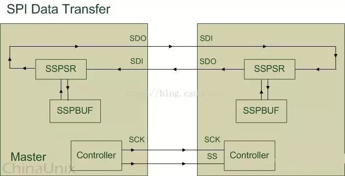
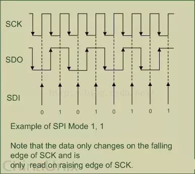
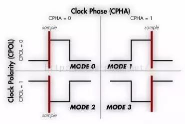
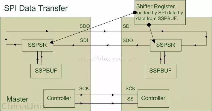
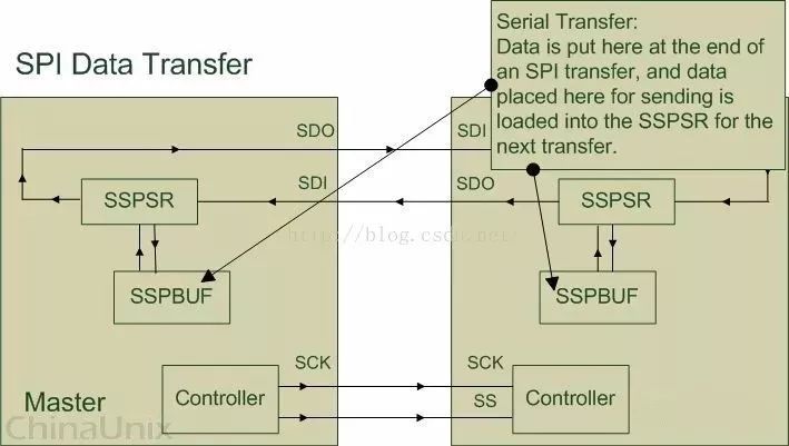
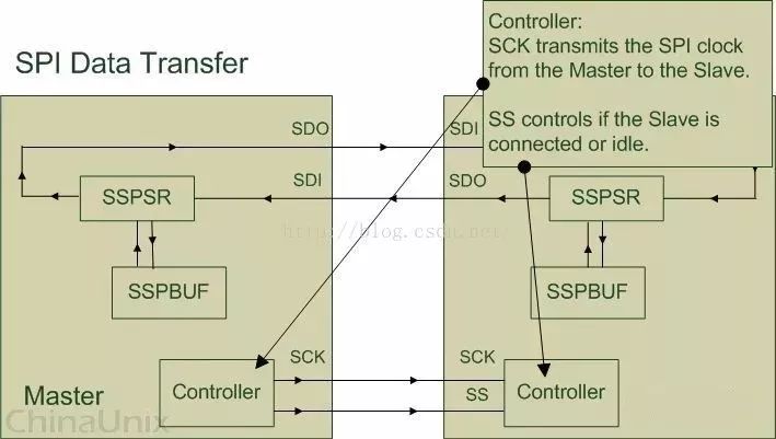
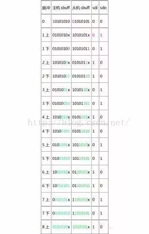
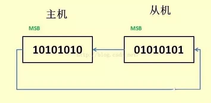
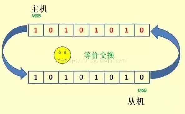
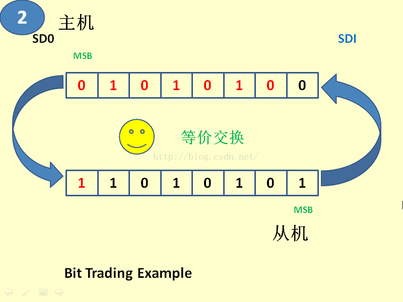
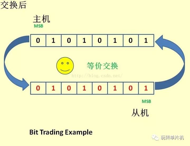
SPI, short for Serial Peripheral Interface, is a communication protocol that enables data exchange between microcontrollers and peripheral devices. Initially developed by Motorola for its MC68HCXX family of processors, SPI has since become widely adopted in various applications such as EEPROMs, flash memory, real-time clocks, ADCs, and digital signal processors. The SPI interface is known for its high-speed, full-duplex, and synchronous nature, using only four pins (SCK, MOSI, MISO, and SS/CS) to facilitate communication. This design helps save pin count on the chip, making it ideal for compact PCB layouts. Due to its simplicity and efficiency, an increasing number of chips now integrate this protocol. SPI operates in a master-slave configuration, where the master device controls the communication. A single master can communicate with multiple slave devices by providing a clock signal through the SCK pin and managing the SS/CS pin to select the active slave. The slave device relies entirely on the master's clock signal, meaning it cannot generate or control the clock itself. Without the clock, the slave will not function correctly. In SPI, data is transferred synchronously based on the clock signal generated by the master. The clock signal determines when data is sampled and sent, ensuring both devices are synchronized. The timing is controlled by two parameters: clock polarity (CPOL) and clock phase (CPHA), which define the edge at which data is sampled and shifted. During SPI communication, each clock cycle allows the transfer of one bit of data. Both the master and the slave send and receive data simultaneously. Before any data is exchanged, the master must select the desired slave via the SS/CS pin. If the received data is not read before the next transmission, it may be lost, causing errors in the communication process. Therefore, after sending data, it is common practice to read the received data from the SPI buffer, even if it is dummy data. SPI supports four different modes based on CPOL and CPHA combinations. These modes determine when data is sampled relative to the clock signal. Additionally, data can be transmitted either as Most Significant Bit (MSB) first or Least Significant Bit (LSB) first. SPI is strictly a master-slave system. Every data transfer involves both the master and the slave exchanging data. Sending a byte requires receiving a byte in return, and vice versa. This bidirectional communication ensures that no data is lost during the exchange. The SPI communication mechanism involves several key components within the SPI device. The SSPBUF (Serial Port Buffer) acts as a temporary storage for data being transmitted or received. The SSPSR (Serial Port Register) is a shift register responsible for shifting data into or out of the SSPBUF. The controller manages the configuration of the SPI bus, including the mode of operation and clock settings. The main signals involved are SCK (Serial Clock), SS/CS (Slave Select), SDO/MOSI (Master Out Slave In), and SDI/MISO (Master In Slave Out). These signals work together to enable seamless data exchange between the master and the slave. Timing is crucial in SPI communication. The figure illustrates how data is exchanged between the master and the slave over eight clock cycles. Understanding the concepts of clock polarity (CPOL) and clock phase (CPHA) is essential for proper configuration. These parameters define the behavior of the clock signal and the timing of data sampling. Common terms used in SPI include CPOL (Clock Polarity), CPHA (Clock Phase), SCK (Serial Clock), and Edge (the point where the clock changes state). These terms help describe the timing and behavior of the SPI signal. CPOL and CPHA can each be set to 0 or 1, resulting in four possible operating modes: Mode 0 (CPOL=0, CPHA=0), Mode 1 (CPOL=0, CPHA=1), Mode 2 (CPOL=1, CPHA=0), and Mode 3 (CPOL=1, CPHA=1). Each mode defines when the data is sampled relative to the clock edges. CPOL determines the idle state of the SCK signal. When CPOL=0, the clock is low when idle, and becomes high during active periods. When CPOL=1, the clock is high when idle and goes low during active periods. This setting affects the timing of data sampling. CPHA determines whether data is sampled on the first or second edge of the clock signal. For example, if CPHA=0, data is sampled on the first edge, while CPHA=1 means data is sampled on the second edge. This parameter is critical for ensuring accurate data transfer. To ensure correct communication, the master and slave must be configured to the same mode. The slave’s mode is usually defined in its datasheet, and the master must match this configuration. Some devices allow software configuration of CPOL and CPHA, typically by writing specific values to the corresponding registers. The SSPSR is a shift register that shifts data into or out of the SSPBUF based on the clock signal. The size of each data transfer depends on the Bus-Width and Channel-Width settings. Bus-Width defines the data unit between the address bus and the master, while Channel-Width defines the data unit between the master and the slave. Proper configuration ensures smooth data flow without data loss. The SSPBUF is a buffer that stores data temporarily during transmission. Data is written to the Tx-Data register and then moved into the SSPBUF by the shift register. Similarly, received data is stored in the Rx-Data register. This process ensures that data is properly transferred between the master and the slave. The controller manages the clock and chip select signals to coordinate communication between the master and the slave. The slave waits for the chip select signal from the master before responding to the clock. This signal is typically controlled by the program, which sets the SS/CS pin low to initiate communication and high to end it. SPI uses a ring bus structure involving SS/CS, SCK, SDI, and SDO. Let’s say we want to transmit the 8-bit value 10101010. With rising edge transmission and falling edge reception, the data will be sent on the rising edge of the clock, and the received data will be sampled on the falling edge. After eight clock cycles, the data will have been fully exchanged between the two devices. This example demonstrates how data is exchanged in a simple SPI setup. The upper waveform shows the rising edge, and the lower one represents the falling edge. The SDI and SDO lines are relative to the master device. Understanding this process is key to implementing SPI in real-world applications. STM32 microcontrollers come with built-in SPI support, making implementation straightforward. [cpp] view plaincopy Void SPIInit(void) { SPI_InitTypeDef SPI_InitStructure; // Initialize the connection between SPI and GPIO port FLASH_GPIO_Init(); /*!< Deselect the FLASH: Chip Select high */ CE_High(); /*!< SPI configuration */ SPI_InitStructure.SPI_Direction = SPI_Direction_2Lines_FullDuplex; SPI_InitStructure.SPI_Mode = SPI_Mode_Master; SPI_InitStructure.SPI_DataSize = SPI_DataSize_8b; SPI_InitStructure.SPI_CPOL = SPI_CPOL_High; SPI_InitStructure.SPI_CPHA = SPI_CPHA_2Edge; SPI_InitStructure.SPI_NSS = SPI_NSS_Soft; SPI_InitStructure.SPI_BaudRatePrescaler = SPI_BaudRatePrescaler_8; SPI_InitStructure.SPI_FirstBit = SPI_FirstBit_MSB; SPI_InitStructure.SPI_CRCPolynomial = 7; SPI_Init(SPI1, &SPI_InitStructure); /*!< Enable the sFLASH_SPI */ SPI_Cmd(SPI1, ENABLE); } [cpp] view plaincopy Uint8 Send_Byte(uint8 data) { // Wait until the transmit buffer is empty While(!(SPI1->SR & SPI_I2S_FLAG_TXE)); SPI1->DR = data; // Read the received data While(!(SPI1->SR & SPI_I2S_FLAG_RXNE)); Return SPI1->DR; } [cpp] view plaincopy Uint8 Get_Byte(void) { // Wait until the transmit buffer is empty While(!(SPI1->SR & SPI_I2S_FLAG_TXE)); // Transmit buffer is empty, exit loop SPI1->DR = 0xFF; // Send dummy data // Wait until the receive buffer is not empty While(!(SPI1->SR & SPI_I2S_FLAG_RXNE)); // Receive buffer is not empty, exit loop Return SPI1->DR; } Photovoltaic charge controller,Solar Charging Controller,MPPT Solar Charger Ningbo Taiye Technology Co., Ltd. , https://www.tysolarpower.com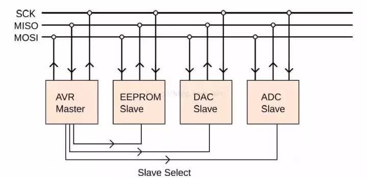
1. Regulation of Charging: The primary function of a solar charge controller is to regulate the charging process. It prevents the Solar Panel from supplying excess current to the battery, ensuring that the battery is charged at an optimal rate.
2. Voltage Regulation: It maintains the battery voltage within safe limits, protecting the battery from overcharging or undercharging. This is crucial for extending the life of the battery.
3. Protection: Solar charge controllers provide protection against common issues such as overcharging, deep discharge, short circuits, and reverse polarity. They can also prevent the battery from being discharged when there's no sunlight.
4. Monitoring: Some controllers offer features like real-time monitoring of voltage, current, and power output, allowing users to track the performance of their solar system.
Choosing the right solar charge controller depends on various factors including the size of your solar panel array, the type and capacity of your battery bank, and your specific power needs. By selecting an appropriate controller, you ensure a reliable, efficient, and long-lasting solar power system.
Deep interpretation of SPI features, mechanisms and drivers and examples
1. Introduction to SPI
2.3 Data Exchange
3.2.3 Clock Polarity
5. STM32 Driver
A solar charge controller, also known as a solar charge regulator, is an essential component in a solar power system designed to regulate the flow of electricity from solar panels to batteries. Photovoltaic charge controller ensures that the batteries are charged efficiently and safely while preventing overcharging, which could damage the batteries.
Functions