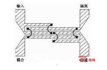
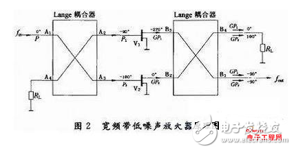
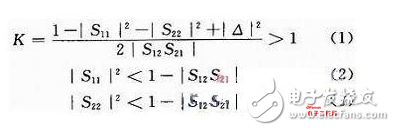
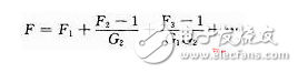
Broadband Low Noise AmpliTIer (BBLNA) is a key component of a receiving system such as communications and measurement and control. Its noise figure, gain, and frequency response characteristics directly affect the main performance of the receiving system. Therefore, in the field of broadband receiving systems, the design of broadband low-noise amplifiers will have very broad market prospects. The power gain of various low-noise devices decreases as the frequency increases, with a regular decrease of approximately 3~5dB per octave. In order to obtain a wider and flatter frequency response characteristic, the gain roll-off must be compensated. However, deliberately reducing the gain of the low frequency band will inevitably make the input and output standing wave ratio worse, and the noise figure will also increase. But for broadband low-noise amplifiers, it is generally impossible to use an isolator to improve the standing wave ratio. In addition, the input and output impedances of low-noise devices also vary greatly with frequency, which increases the complexity of the matching circuit. Although the circuit structure of the wide-band low-noise amplifier has many forms, the balanced amplifier designed with the Lange coupler has the advantage of noise, and its noise figure is similar to that of the single-ended low-noise amplifier. When designing the matching circuit, it can be completely According to the best noise matching design, there is no need to take into account the input and output standing wave ratio. Therefore, a balanced circuit structure is selected for the design of a broadband low-noise amplifier. 1 Design principle The balanced broadband low-noise amplifier consists of two low-noise devices and two Lange couplers. The two low-noise devices and their matching circuit networks are completely the same, reducing the complexity of matching circuit calculations, input and output standing waves Good ratio, low noise, working frequency band up to 1~2 octave. 2Lange coupler The Lange coupler is also called a 90° three-decibel bridge, and its structure is shown in Figure 1. It has a very prominent advantage over other couplers in terms of broadband and tight coupling characteristics. The design idea is to use several coupled lines to be parallel to each other, so that both sides of the line are coupled to achieve tight coupling, and to improve the bandwidth by compensating the phase velocity. Almost all commonly used microwave circuit simulation software has typical models to facilitate design. 3 design principles The schematic diagram of the balanced broadband low-noise amplifier is shown in Figure 2. If the power and phase of the input RF signal fin are P and 0° respectively, it is equally divided into two parts, P1 and P2, by the Lange coupler. The phase of P1 is -90°, and the phase of P2 is -180°, which are respectively amplified by two paired low-noise devices. Because the matching circuit is the same, the gain G is the same, and the transmission phase shift is changed by 180°. The amplified two signals are GP1 and GP2, the phase of GP1 is -270°, and the phase of GP2 is 0°. After the two signals are combined by the coupler, the magnitudes of GP1 and GP2 at port B4 are equal, the phase difference is 180°, and there is no power output; at port B1, GP1 and GP2 have the same phase, and the two parts of power are superimposed to output fout, the magnitude of which is GP1+GP2 =G(P1+P2)=GP. That is, in an ideal state, the gain of the balanced broadband low-noise amplifier is equal to the gain of a single low-noise device. The use of a balanced circuit structure has the following advantages: (1) Since each low-noise device only undertakes half of the power amplification, the 1dB compression point of the amplifier output power will increase by 3dB, the corresponding dynamic range will also increase by 3dB, and the third-order intermodulation will be improved by about 6dB. (2) The port standing wave ratio has been greatly improved. It is now assumed that the reflection coefficients of V1 and V2 are equal. The RF signal fin is input from the coupler A1 port, and is divided into two parts and output from the A2 and A3 ports. The reflected power of the A2 port is returned To port A1, the total path phase shift is -180°; the reflected power of port A3 returns to port A1, and the total path phase shift is -360°. Obviously the reflected power of the two parts are equal, and the phases are opposite and cancel out. Therefore, at port A1 There is no reflected power. In addition, the reflected power of V1 and V2 are superimposed on the A4 port, and a 50Ω matching load RL is needed for absorption. Through the phase shifting effect of the coupler, the port standing wave ratio is constant at 1. (3) The stability of the amplifier is improved, and the judgment conditions for the stability of the amplifier are as follows: In the formula: △=S11S22-S12S21, K is the stability factor. When the above three conditions are met at the same time, the amplifier is absolutely stable. It can be proved that the stability judgment coefficient K of the balanced amplifier is always greater than 1. In Figure 2, the A1 port and the B1 port are theoretically non-reflective, and there is no self-oscillation that may be caused by the reflection of the signal source or load. Although a single low-noise device itself has potential instability in the low frequency band, as long as the matching circuit is designed well, the A1 port and the B1 port are absolutely stable. This feature is very important in a wideband receiving system, especially when the antenna is matched with the amplifier, the effect will be more obvious. (4) The lowest noise figure of a balanced amplifier is basically the same as that of a single-ended amplifier, but when designing the matching circuit, the design can be completely designed according to the best noise matching to obtain the ideal minimum noise matching without taking into account the standing wave ratio. In the narrow-band low-noise amplifier, the common structure of the DC bias power supply lead-in line is a λg/4 high-impedance microstrip line, and its terminal adopts a sector line or a capacitor to short-circuit the high frequency. The available operating frequency band of this structure is no more than 40% ~50% bandwidth. Therefore, in the broadband low-noise amplifier circuit, it is impossible to use this form of bias lead-in. The bias lead-in of the microstrip line center jumper type can be used, that is, the jumper is soldered on the center axis of the microstrip. In an ideal state, there is no electric field distribution in the space directly above the center of the microstrip line. The distance between the solder joint on the outer end of the jumper and the edge of the microstrip must be at least greater than the thickness of the substrate to ensure that the solder joint is outside the electric field. Since the diameter of the jumper has a weak influence on the inductance, and the length has a greater influence on the inductance, it needs to be accurately controlled. The jumper wire can be properly separated from the surface of the substrate to reduce the influence of the floor on the inductance. In addition, low-frequency filtering and inter-stage low-frequency decoupling capacitors of the power supply should be considered. The decoupling and bypass circuits should be large enough to avoid low-frequency oscillations. The DC blocking capacitors in the microstrip circuit try to use wide-band surface-mount capacitors with high Q value, high stable temperature coefficient, no resonance and low loss, such as the C06 series products of DLI Corporation in the United States. The lateral width of the shielded box should be less than half the wavelength of the highest operating frequency to avoid waveguide transmission effects in the internal space of the box. The microstrip substrate should be well grounded, and the number of fixing screws should be relatively large. It is best to metalize the wall of the screw hole for grounding. When debugging, stick the corresponding frequency band absorbing material on the inner surface of the upper cover of the box body to reduce the fluctuation of in-band gain caused by spatial coupling. Broadband low-noise amplifiers also need to be designed for electromagnetic compatibility. First, use a core capacitor with a feed-through filter to filter the power line entering the shielding box to reduce the crosstalk problem caused by the power line; secondly, the amplifier needs to be resolved. Matching of ports to ensure compatible work when integrated into the receiving system; finally, electromagnetic shielding measures need to be taken to the box body to reduce interference problems caused by electromagnetic radiation. Strengthening the electromagnetic compatibility work in the research and development stage is conducive to the products passing the corresponding standard electromagnetic compatibility test. 4 design example simulation According to the development requirements of a certain task, it is necessary to design a low noise amplifier that works in the L/S band. The main technical indicators include: working frequency 1.2~2.5GHz; P-1dB≥10dBmW; gain G≥32dB; noise figure Nf≤1.1dB The input and output standing wave ratio is not more than 1.5. According to previous engineering experience, two NE42484A low-noise devices produced by NEC are selected for balanced circuit design. The gain of this circuit obviously cannot meet the index requirements, and a high gain and noise level needs to be added. A lower amplifier with an in-band matching circuit, such as the SAN-386 internal matching transistor produced by Stanford. According to the multi-stage amplifier noise calculation formula: Where: F is the total noise figure of the two-stage amplifier, F1 and F2 are the noise figure of the first and second stage respectively, and G1 and G2 are the gains of the first and second stage respectively. It can be clearly seen from this formula that the noise figure after cascading mainly depends on the noise figure of the first stage amplifier, and the greater the gain of the first stage, the smaller the contribution of the latter stage to the total noise figure. The S-parameters of the two NE42484A FETs should be selected as consistent as possible. The microstrip substrate is a composite dielectric substrate with a dielectric constant of 9.2 and a thickness of 1mm. The simulation circuit topology is established using ADS software, and the form of the matching circuit is microstrip impedance transformation. Type matching method, which is equivalent to a series of several microstrip lines in form. According to the S parameters of NE42484A FET and SAN-386 transistor, the simulation optimization design is carried out. The commonly used optimization methods are divided into stochastic optimization and gradient optimization. The stochastic method is usually used for large-scale search, and the gradient method is used for local convergence. A small number of variable parameters can be set during optimization, and the various indicators of the amplifier are optimized step by step. First, use the random method of 100 to 200 steps to optimize, and then use the gradient method of 20 to 30 steps to optimize. Generally, the optimal result. The simulation results are shown in Figure 3. In the 1.2~2.5GHz working frequency band, the 1dB compression point of output power has been guaranteed when the device is selected; the in-band gain is between 35~37dB; the noise figure is not more than 0.8dB; the input and output are stable. The wave ratios are all less than 1.5. The simulation analysis results show that this design scheme can meet the development requirements. Draw the microstrip circuit board through the optimized circuit topology by simulation, pay attention to adding isolation islands in the matching microstrip line to facilitate the change of the size of the microstrip line during debugging and obtain better performance; a large area around the circuit is attached Copper, and leave a denser metalized grounding vias to enhance the grounding performance of the circuit, as shown in Figure 4. The figure is marked with V1, V2 is the two NE42484A field effect transistors to be welded, and V3 is the SAN-386 transistor to be welded. ' In the production and debugging process of the amplifier, it was found that there are two important links that need attention, one is the guarantee of the processing technology; the other is the debugging of the power supply bias inductance. Bonding jumpers are required between the coupling lines of the Lange coupler, as shown in Figure 1. The test proves that the microstrip circuit board is gold-plated and the gold wire bonding process can ensure the reliability and accuracy, and the coupling line uses a single jumper or The performance indicators of multiple jumpers are basically unchanged, so it is recommended to use more than two jumpers in parallel to improve reliability in actual use. If there is no gold wire welding technology in the process conditions, you can also use the same topology and choose the Lange coupler produced by a professional manufacturer, such as the miniaturized surface mount device of Anaren. The power supply bias inductance needs to be manually formed. During debugging, the inductance can be changed by fine-tuning the coil spacing to achieve the best matching of the circuit. After the debugging is completed, it is reinforced with silicone rubber to improve reliability. After the completion of the amplifier debugging, the actual test of the required indicators was carried out. Within the working frequency band of 1.2~2.5GHz, the gain is between 33~35dB, which is about 2dB smaller than the simulation result; the noise figure is not more than 1dB, which is less than The simulation results are about 0.2dB larger; the input and output standing wave ratios are basically consistent with the simulation results. Therefore, all indicators of the wide-band low-noise amplifier meet the requirements of the development task. 5 Conclusion Using the broadband characteristics of the Lange coupler to design a balanced broadband low-noise amplifier, ideal noise matching can be obtained, without taking into account the standing wave ratio, and the reliability and stability of the amplifier are also relatively good, and through the simulation and test of the design example The results verified the corresponding indicators. Ccd Fix- Mounted Scanner, Fixed Mount Barcode Scanner,Fixed Mount Barcode Barcode,Wall Mounted Barcode Scanner Guangzhou Winson Information Technology Co., Ltd. , https://www.winsonintelligent.com