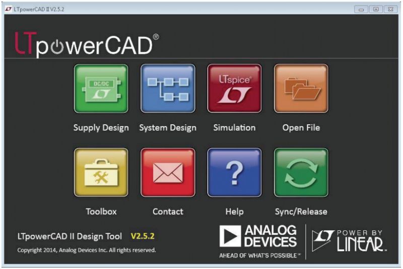
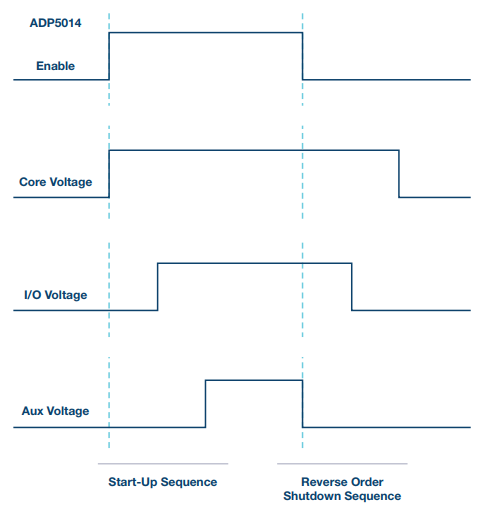
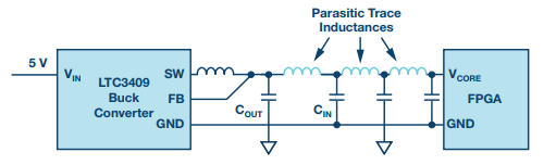
Designing an excellent power management solution for FPGA applications is not a simple task, and there are many related technical discussions. The contents of "FPGA Power Management" that Xiaobian will share for you today have two main purposes - ☞ Find the right solution and choose the most suitable power management product ☞ How to optimize practical solutions for use in FPGAs Finding the right power solution Finding the best solution for powering an FPGA is not simple. Many vendors market certain products in the name of powering FPGAs. What are the specific requirements for the selection of a DC-DC converter that powers an FPGA? In fact, not much. In general, all power converters can be used to power the FPGA. Recommended products are often based on the fact that many FPGA applications require multiple voltage rails, such as for the FPGA core and I/O, and additional voltage rails may be needed for DDR memory. PMICs (power management integrated circuits) that integrate multiple DC-DC converters into a single regulator chip are often preferred. One popular way to find a good power solution for a particular FPGA is to use the existing power management reference designs provided by many FPGA vendors. This is a good way to get started with optimization. But such designs often need to be modified because FPGA systems usually require additional voltage rails and loads, which also require power supply; Adding something to the reference design is often necessary; The input power to the FPGA is not fixed, and the input voltage depends to a large extent on the actual logic level and the design implemented by the FPGA. After completing the revision of the power management reference design, it will look different from the original reference design. Some may argue that the best solution is to not use the power management reference design at all, but to directly input the required voltage rails and currents into the power management selection and optimization tools, such as ADI's LTpowerCAD. Figure 1. Selecting a suitable DC-DC converter through LTpowerCAD tool to power the FPGA. LTpowerCAD can be used to provide power solutions for various voltage rails. It also offers a series of reference designs to get designers to get started quickly. LTpowerCAD can be downloaded for free from the Analog Devices website. How to Optimize a Real-World Solution for FPGAs Once the power supply architecture and individual voltage converters are selected, suitable passive components need to be selected to design the power supply. When doing this, keep in mind the special load requirements of the FPGA - Current demand  Voltage rail timing control Monotonically rising voltage rails Fast power transients Voltage accuracy FPGA input capacitance The actual current consumption of the FPGA depends to a large extent on the usage. Different clocks and different FPGA content require different power. Therefore, the final power supply specifications of a typical FPGA design will inevitably change during the design of the FPGA system. The power estimation tool provided by the FPGA manufacturer helps to calculate the power level required for the solution. Obtaining this information can be very useful before building the actual hardware. However, in order to obtain meaningful results using such power estimation tools, the design of the FPGA must be finalized, or at least nearly finalized. Normally, engineers consider the maximum FPGA current when designing power supplies. If you finally find that the actual FPGA design requires less power, designers will reduce the power supply. Many FPGAs require different power supply rails to power up in a specific order. The supply of the core voltage often needs to be earlier than the supply of I/O voltage, otherwise some FPGAs will be damaged. To avoid this situation, the power supply needs to be powered up in the correct order. Using the enable pin on a standard DC-DC converter, simple power-up sequencing can be easily implemented. However, device shutdown usually also requires timing control. Only implementing the enable pin timing control makes it difficult to achieve good results. A better solution is to use a PMIC with advanced integrated timing control, such as the ADP5014. The special circuit module shown in red in Figure 2 supports adjusting power-up and shut-down timings. Figure 2. The ADP5014 PMIC integrates support for flexible control power-up/shutdown timing. Figure 3 shows the timing control implemented using this device. The time delay for power-up and power-down sequencing can be easily adjusted with the delay (DL) pin on the ADP5014. Figure 3. Start and Shutdown Sequence of Multiple FPGA Supply Voltages. If multiple separate power supplies are used, adding the timing control chip can achieve the desired power-up/power-down sequence. One example is the LTC2924, which controls the DC-DC converter's enable pin to turn the power on and off, and it also drives the high-side N-channel MOSFET to connect and disconnect the FPGA from a voltage rail. In addition to voltage sequencing, monotonic rises in voltage may also be required during startup. This means that the voltage only rises linearly, as shown by the voltage A in Figure 4. The voltage B in this figure is an example of a non-monotonic rise in voltage. This occurs when the load starts to draw a large current when the voltage rises to a certain level during startup. One way to prevent this is to extend the soft-start time of the power supply and select a power converter that can quickly provide a large amount of current. Figure 4. Voltage A rises monotonically and voltage B does not rise monotonically. Another feature of the FPGA is that it starts to draw large amounts of current very quickly. This can cause high load transients on the power supply. For this reason, many FPGAs require a large amount of input voltage decoupling. Ceramic capacitors are used very closely between the VCORE and GND pins of the device. Up to 1 mF is very common. This high capacitance helps reduce the need for very high peak currents in the power supply. However, many switching regulators and LDOs specify the maximum output capacitance. The input capacitance requirement of the FPGA may exceed the maximum output capacitance allowed by the power supply. Power supplies do not like very large output capacitors for two reasons - During startup, the output capacitance of the switching regulator appears to be short-circuited. There is a solution to this problem. A longer soft-start time allows the voltage on the large capacitor group to steadily increase and the power supply will not enter the short-circuit current limit mode. Figure 5. Input capacitance requirements for many FPGAs. This capacitance value becomes part of the regulation loop. Converters with integrated loop compensation do not allow excessive output capacitance to prevent regulator loop instability. Using a feed-forward capacitor on the high-side feedback resistor can often affect the control loop, as shown in Figure 6. Figure 6. Using a feed-forward capacitor can adjust the control loop when no loop compensation pin is available. The development tool chain (including LTpowerCAD, especially LTspice) is very helpful for power supply load transients and startup behavior. The tool can be well modeled and simulated to effectively decouple the large input capacitance of the FPGA from the output capacitance of the power supply. Figure 6 shows this concept. Although the POL (load side) power supply is often located close to the load, there are often PCB traces between the power supply and the FPGA input capacitance. When there are multiple FPGA input capacitors next to each other on the board, those capacitors furthest from the power supply have less impact on the power transfer function because there is not only some resistance but parasitic trace inductance between them. These parasitic inductances allow the input capacitance of the FPGA to be greater than the maximum limit of the output capacitance of the power supply, even if all capacitors are connected to the same node on the board. In LTspice, parasitic trace inductance can be added to the schematic and these effects can be simulated. When the circuit modeling contains enough parasitic components, the simulation results are close to the actual results. Figure 7. Parasitic decoupling between the output capacitance of the power supply and the input capacitance of the FPGA. The voltage accuracy of the FPGA power supply is usually very high. The 3% change tolerance band is quite common. For example, to keep the 0.85 V Stratix V core voltage rails within a 3% voltage accuracy window, all tolerance bands are required to be only 25.5 mV. This small window includes voltage changes and DC accuracy after load transients. Similarly, for such stringent requirements, the available power tool chains including LTpowerCAD and LTspice are very important in the power supply design process. In order to provide a large current quickly, the input capacitance of the FPGA is usually a ceramic capacitor. This type of capacitor is suitable for this purpose, but it needs to be carefully chosen so that its true capacitance does not drop with the DC bias voltage. Some ceramic capacitors, especially the Y5U type, when the dc bias voltage is close to its maximum rated dc voltage, its true capacitance will be reduced to only 20% of the nominal value. Schottky Diode,Schottky Barrier Diode,Schottky Diode Forward Voltage,Sic Schottky Diode Shenzhen Kaixuanye Technology Co., Ltd. , https://www.iconlinekxys.com
 Current requirements
  Voltage rail timing control
 Monotonically rising voltage rails
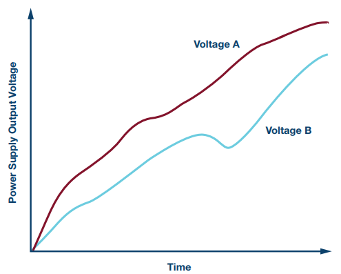
 Fast power transients
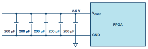

 Voltage accuracy
  FPGA input capacitance