Shenzhen Ousida Technology Co., Ltd , https://en.osdvape.com
A folding mixer suitable for operation at low supply voltages
Currently, wireless communication devices are trending towards low voltage, low power consumption, low noise, and high linearity. As a crucial component in the transceiver, the mixer significantly influences these performance aspects. With advancements in microelectronics, the gate length of CMOS devices has been reduced, along with the overdrive voltage, enabling the design of low-voltage and low-power RF circuits. However, this also imposes limitations on further lowering the operating voltage. Therefore, circuit designers have increasingly focused on optimizing circuit topologies, making low-voltage RF circuits a prominent research area.
The traditional Gilbert mixer consists of a transconductance stage, a switching stage, and a load stage stacked vertically. In this configuration, all DC current flows through these stages. Both the transconductance and switching stages require a turn-on voltage (Von), while the load stage also experiences a voltage drop (VRL). This results in a minimum supply voltage of Vdd,min = 2Von + VRL. If a lower supply voltage is used, it may not ensure that all transistors operate in saturation, limiting the mixer’s ability to meet low-voltage requirements. Several studies have proposed solutions, such as eliminating the tail current transistor in [2–3] or using a folded structure instead of a stacked one in [4–11].
In literature [8], a comparison between folded and stacked structures is presented. The folded structure introduces two RF interrupt circuits and a coupling capacitor, allowing the transconductance stage to be separated from the DC paths of the switching and load stages. This enables independent operation and reduces the required supply voltage to Vdd,min = Von + VRL. However, RF interrupt circuits typically use LC resonant networks, which increase layout area and noise. To address this, this paper presents a new folded mixer topology that avoids large inductors. Operating at 1.2 V, the circuit achieves low voltage, low power, low noise, and high linearity.
**1 Circuit Design and Analysis**
**1.1 Circuit Topology**
The folded mixer topology designed in this paper is shown in Figure 1. M1 to M4 form the transconductance stage, M5 to M8 are the switching stage, and RL represents the load resistance. The RF input is connected to a matching network, and the IF output is buffered by a source follower.
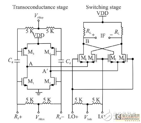
*Figure 1: AC-coupled folding mixer topology*
The transconductance stage employs current multiplexing technology, with NMOS transistors (M1, M2), PMOS transistors (M3, M4), and a DC blocking capacitor Cd forming an AC-coupled complementary structure. The outputs (points A and A') are connected to the sources of the switching transistors. Since the transconductance stage is directly connected to the power supply, the DC current through M1 and M2 is split into two parts—some through M3 and M4, and others through the switching transistor and load resistor. This helps achieve a low supply voltage.
Due to the small current in the switching and load stages, the flicker noise from the switching transistor is reduced, and the load resistance can be increased, improving the conversion gain. Thus, the circuit satisfies low-voltage requirements while maintaining good performance under low power conditions.
**1.2 Transconductance Circuit Design**
Figure 2 shows several transconductance circuit configurations for the folded mixer. In Figure 2(a), the drain of the NMOS transistor M1 is connected to a load resistor R. The current In of M1 splits at point A, with part flowing through the switch tube (Is) and the rest through the load resistor (IR). However, this design allows some RF signal to leak to AC ground via the resistor R.
To reduce RF signal loss, the resistor R must be increased, which lowers the DC voltage at node A. Under low power supply voltage, this may prevent M1 from operating in saturation. To solve this, the load resistor R is replaced with an active load, as shown in Figure 2(b). However, the PMOS transistor here only increases the impedance between node A and the power supply. If the gates of M1 and M2 are connected to form a CMOS inverter, M2 can increase the impedance and amplify the RF signal, as shown in Figure 2(c), effectively preventing RF signal leakage through M2 to AC ground.
As illustrated, Is = In + Ip, and the total transconductance is gm = gm_n + gm_p (where gm_n is the transconductance of the NMOS and gm_p is that of the PMOS). Thus, the CMOS inverter improves the mixing conversion gain.
Next, we analyze the DC operating condition of the structure. The gates of M1 and M2 are biased with the same voltage Vrfdc. Assuming Vt is the threshold voltage of the MOS transistor, Vovn is the overdrive voltage of M1, and Vovp is that of M2, we have:
Vovn = Vrfdc - Vt
Vovp = Vdd - Vrfdc - Vt
Therefore, the minimum supply voltage is:
Vdd,min = Vovn + Vovp + 2Vt