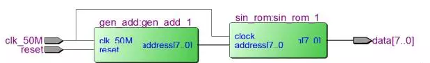
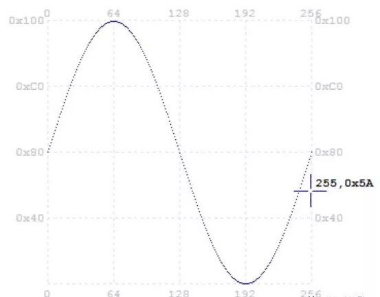
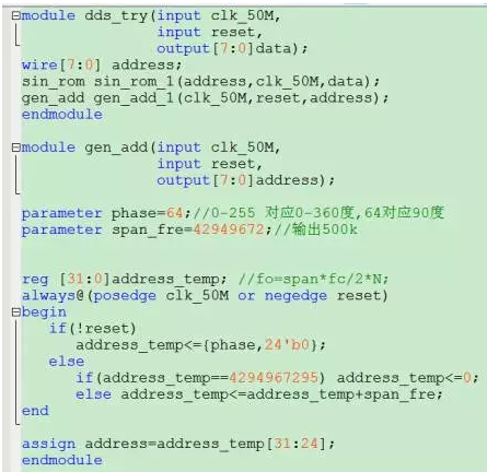
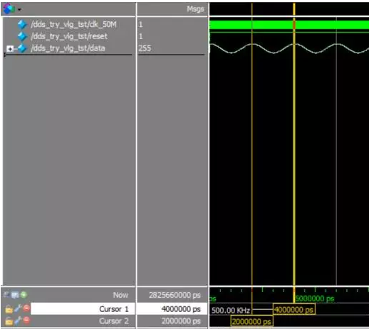
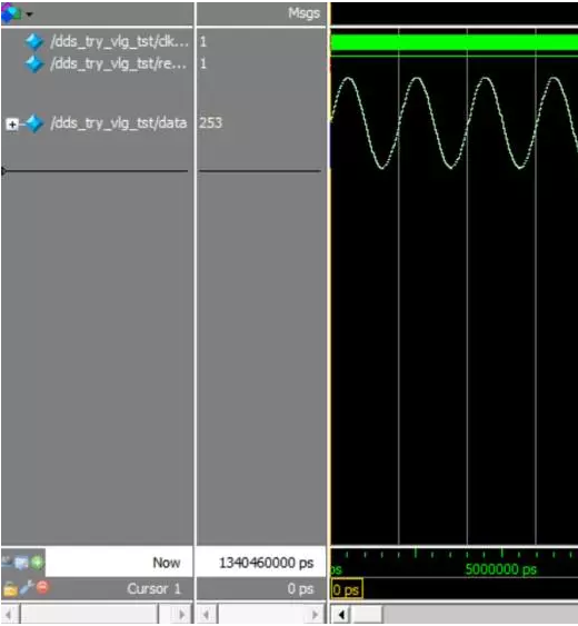
DDS is the acronym for Direct Digital Synthesizer and is a key digital technology. Compared with traditional frequency synthesizers, DDS has the advantages of low cost, low power consumption, high resolution and fast switching time. First of all, to generate a real analog signal, you need to connect to the A / D converter chip, this time mainly to generate the digital signal sent by the FPGA (viewed in analogim in analog). First look at the overall connection diagram: The sin_rom module is a rom that stores sinusoidal waveform data (rom calls quartusip core), depth 256, width 8 bits, we use to generate a good mif file (can be generated by mif_make2010 software, can also be generated using c language matlab but pay attention to the file Format) to initialize the rom, if we use mif_make2010 to generate the mif file, the waveform is as follows: The row coordinate is 0-255, which means 256 storage units of rom, the ordinate indicates the value of each storage unit, the peak is 0xFF; the trough is 0x00, that is, we read from the first address of rom in turn, After reading all the time, the data read from the rom is the digital representation of the sinusoidal waveform. Therefore, in the program, we only need to control the generation of the address to achieve the purpose of phase modulation and frequency modulation, so the gen_add module is set. Phase modulation principle: Since the phase corresponding to 0-255 units is 0-360 degrees, we only need to adjust the unit of the initial phase to reach the purpose of phase modulation. For example, if the initial unit is 0, then our waveform is standard. Sine wave, if our initial unit is 64, then our waveform is a cosine wave. Frequency modulation principle: We can adjust the waveform frequency by adjusting the frequency of the address generation. If we have a clock of 50M, each clock rising edge reads a data from the rom. Since the sin waveform of one cycle is composed of 256 points, we are equivalent to 256 clocks to generate a complete sin wave, that is, the period is 256*. (1/50M); frequency is 50M/256; From the frequency expression we can see that the frequency of the waveform is related to the clock, and the second is related to the number of stored rom units. We use 256 units above, so the generated frequency is 50M/256=195.3Khz, which is We sequentially read the data from the rom, that is, the frequency of each clock plus one generated. If we add 2 (step) to each clock address, our generated frequency is twice the original, that is, 2* 50M/256=195.3*2. But we think about it. If our rom depth is 256, the highest frequency resolution is 50M/256 or 195.3Khz, and the frequency we generate can only be an integer multiple of 195.3Khz, which is a bit unacceptable. We naturally think that we can increase the number of rom digits to improve the indexing rate. Of course, but our rom is fixed in advance. Is there any other way? If we set a 32 register address_temp, we only pass the first eight bits of address_temp to the rom to read the data, which is equivalent to slowing down the rate of change of the address, but we actually improve the frequency resolution, the current resolution The rate is 50M/2^32=0.011hz. Similarly, the frequency we generate can only be a multiple of 0.011hz, but we can think that any integer can be a multiple of 0.011. If the step size is span_fre, the frequency generated is span_fre*50M. /2^32; This is somewhat similar to the previous application (3) precision crossover, in fact its principle comes from this. In the same way, we can adjust the step size according to the frequency. The procedure is as follows: The simulation results are as follows: From the result, we can see that the starting phase is 90 degrees, that is, the cos waveform, (although we store the data of the sin waveform in rom), the frequency is 500k. Note that the display format of data is set to an unsigned analog quantity. When we change the phase to 0, the result is as follows: It can be seen that the starting phase is 0 degrees at this time, which is the sin waveform. PTC Thermistor for Overcurrent Protection for Telecom PTC Thermistor ,Thermistor,Thermistor for Overcurrent Protection ,PTC Thermistor YZPST YANGZHOU POSITIONING TECH CO., LTD. , https://www.cnpositioning.com