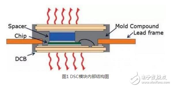
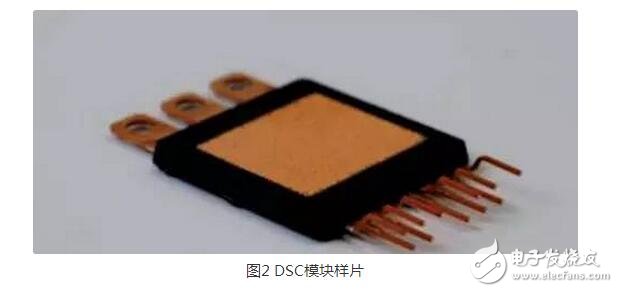
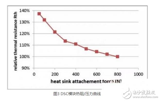
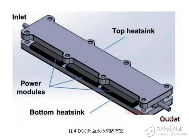
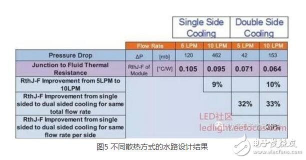
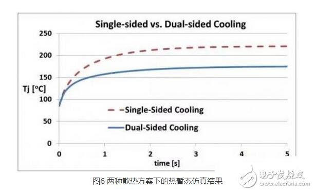
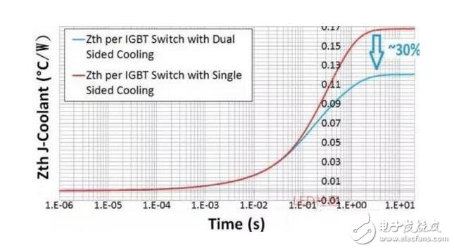
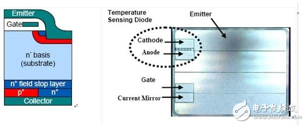
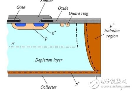
IGBT (Insulated Gate Bipolar Transistor), insulated gate bipolar transistor, is a composite fully controlled voltage-driven power semiconductor device composed of BJT (bipolar transistor) and MOS (insulated gate field effect transistor), which has both MOSFETs. The advantages of both the high input impedance and the low turn-on voltage drop of the GTR. The GTR saturation voltage is reduced, the current carrying density is large, but the driving current is large; the MOSFET driving power is small, the switching speed is fast, but the conduction voltage drop is large, and the current carrying density is small. The IGBT combines the advantages of the above two devices, with low driving power and reduced saturation voltage. It is very suitable for converter systems with DC voltages of 600V and above, such as AC motors, inverters, switching power supplies, lighting circuits, traction drives, etc. The IGBT module is a modular semiconductor product that is packaged by IGBT (Insulated Gate Bipolar Transistor Chip) and FWD (Freewheeling Diode Chip) through a specific circuit bridge; the packaged IGBT module is directly applied to the inverter and the UPS is uninterrupted. On the power supply and other equipment; IGBT module has the characteristics of energy saving, convenient installation and maintenance, and stable heat dissipation; most of the products currently on the market are such modular products. Generally speaking, IGBT also refers to IGBT modules; with the promotion of energy conservation and environmental protection concepts Such products will become more and more common in the market; IGBT is the core device of energy conversion and transmission, commonly known as the "CPU" of power electronic devices, as a national strategic emerging industry, in rail transit, smart grid, aerospace, It is widely used in electric vehicles and new energy equipment. Infineon's German team and the US team (formerly IR team) published two related designs and test results for double-sided water-cooled IGBT modules. The original title is as follows “Dual-sided Cooling for AutomoTIve Inverters – PracTIcal ImplementaTIon with Power Module†From the application point of view, the development of double-sided water cooling technology (DSC) is based on the application considerations of new energy vehicles (pure electric and hybrid), mainly to solve the problem of power density of vehicle inverters. Figure 1 shows the basic structure. Compared with the existing IGBT module, the DCB on the upper layer of the chip constitutes a second heat dissipation channel for improving the heat dissipation effect of the module. In the sample photo of Figure 2, the module is small in size, the top and bottom are directly in contact with the heat sink through the DCB ceramic substrate, and the strong and weak terminals are distributed on the front and rear sides of the chip. As a double-sided water-cooling module, the mechanical consistency of the plastic sealing material at different temperatures must first be ensured. The surface roughness of the module at 22 and 150 degrees Celsius is good, and the moisture resistance is also excellent. Due to the increase of the heat dissipation channel at the top of the module, the heat dissipation effect is increased by 70%. It should be noted that the thermal resistance value has a great influence on the surface. To achieve the best thermal resistance, the pressure of 800N really scares the author. . Due to the removal of the copper backplane in the conventional design, the heat capacity of the module is significantly reduced, and the thermal coupling performance is greatly improved, and the chip temperature near the heat source is basically high. At the same time, the new DSC module is accompanied by a significant reduction in parasitic inductance and package resistance, with a parasitic inductance of only 13nH. In addition, the module also integrates current and temperature sensors to facilitate chip current and temperature detection. This is not particularly different from conventional chips. Current sensing is basically in the range of 100 millivolts. Compared with the work of the German team, the research focus of the former IR team is on the implementation and performance testing of the water cooling solution. Figure 4 shows the corresponding water-cooled heat sink solution. The inside of the radiator is still using the classic Pin-Fin cooling solution. The focus of the water-cooling design includes the constant flow rate and the optimized design of the pin shape and size under the limitation of the heat dissipation flow family. Based on the same total flow assumption, double-sided water cooling can reduce thermal resistance by 32% compared to single-sided water cooling, while the water pressure drop is only 35%. At the same time, for double-sided heat dissipation, only a 27.5% increase in pressure can achieve double the total heat dissipation flow of single-sided water cooling. The simulation results show that the module with a temperature of 220 degrees Celsius under single-sided water cooling adopts double-sided water cooling and the temperature is only 175 degrees Celsius. For this double-sided heat dissipation, the temperature measurement needs to be modified, such as adding corresponding holes and fixture fixing. The results of the thermal test also confirm the previous design and simulation results, in which the steady-state thermal resistance will reach a 30-40% reduction. At the same time, it can be found that the thermal time constant of the module is only 1.5s, which is much smaller than the conventional IGBT module with copper backplane. Finally, the power-on experiment shows that under the same conditions, after double-sided water cooling, the output power can be increased by more than 30%. The author also predicts that if a more optimized water-cooled design is used, the current capability of the inverter can be increased by 50% or more. IGBT is an ideal switching device in the field of power electronics. Various new structures, new processes and new material technologies are still emerging, which promotes the development of IGBT chip technology. Its power consumption is continuously reduced, and the working junction temperature is continuously rising from 125. °C is raised to 175 ° C and moved to 200 ° C, and the body diode can be integrated on the chip to form a reverse-conducting IGBT (RC-IGBT / BIGT), no need to anti-parallel freewheeling diode, in the same package size, the module can be The current is increased by 30%, and the current and temperature sensors can be integrated into the chip to realize intelligent chip, as shown in the figure. By isolating the edge structure of the IGBT chip, an IGBT (RB-IGBT) with bidirectional blocking capability can be formed, which eliminates the need for series diodes in bidirectional switching applications, and has smaller leakage current and lower loss. The super juncTIon technology breaks the limit relationship between the on-voltage drop and the withstand voltage of conventional silicon devices (RonâˆVB2.5), which can greatly reduce the power consumption of the device and has been successfully applied to MOSFETs. Applying this technology to IGBTs can further reduce power consumption and has received widespread attention. The main difficulty of super-junction IGBT is process realization. In order to reduce the process difficulty, various "semi-super-junction" structures have been proposed to achieve a compromise between performance and process. At the same time, the level of IGBT technology is also increasing, and many advanced process technologies such as ion implantation and fine lithography are applied to IGBT manufacturing. The minimum feature size in the IGBT chip manufacturing process has ranged from 5um to 3um to 1um, even to sub-micron levels. The use of a fine manufacturing process can greatly increase the power density, while reducing the junction depth and reducing the high-temperature diffusion process, making it possible to manufacture IGBTs using silicon wafers of 12 inches or larger. With the development of thin-film and ultra-thin processing, Infineon has produced chip samples with a thickness of only 40um on 8-inch silicon wafers, and it is expected to be applied in the near future. In addition, the development of new materials such as wide bandgap semiconductor materials technology can achieve lower power consumption, higher power capacity, higher operating temperature devices, of which SiC has become the main research direction of current high power semiconductors, and in monopole Commercialization has been achieved on devices, and progress has been made in the research of bipolar devices such as IGBTs. At present, IGBTs are mainly limited by defects in manufacturing processes and substrate materials, such as channel mobility and reliability, low current gain, and growth of highly doped P-type substrates. In the future, with the development of material epitaxy, SiC IGBTs A breakthrough will be achieved. With the continuous development of IGBT chip technology, the highest working junction temperature and power density of the chip continue to increase, and the IGBT module technology should also be adapted. In the future, IGBT module technology will continue to improve on the back side of the chip and the front electrode interconnection. It is expected to combine advanced packaging concepts and technologies such as solderless, wireless bonding and linerless/substrate, and the upper and lower surfaces of the chip. The fixing and electrode interconnection are realized by sintering or crimping, and more other functional components, such as temperature sensor, current sensor and driving circuit, are integrated inside the module, and the power density, integration degree and intelligence of the IGBT module are continuously improved. In this paper, the technical status of IGBT chips is analyzed from three aspects: IGBT body structure, back collector region structure and front MOS structure. At present, IGBT chips generally adopt planar gate or trench gate structure, and use soft through-through structure and transparent collector region structure. Technology, as well as a variety of enhanced technologies to improve overall performance and long-term reliability. The high-voltage IGBT module technology is still based on the standard solder-type package. The medium-low voltage IGBT module products have many new technologies, such as sintering instead of soldering, pressure contact instead of wire bonding, and linerless/substrate packaging. In the future, IGBTs will continue to develop in the direction of integration, intelligence and miniaturization. Digit Segment Led Display,Washing Machine Display,Smd Led Display,Bar Segment Led Display Wuxi Ark Technology Electronic Co.,Ltd. , https://www.arkledcn.com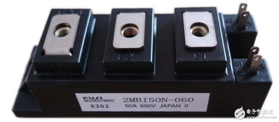
What is an IGBT? How to use this module to achieve "double-sided water cooling", what is the future development trend of IGNT?
What is an IGBT?