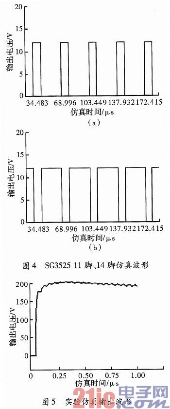
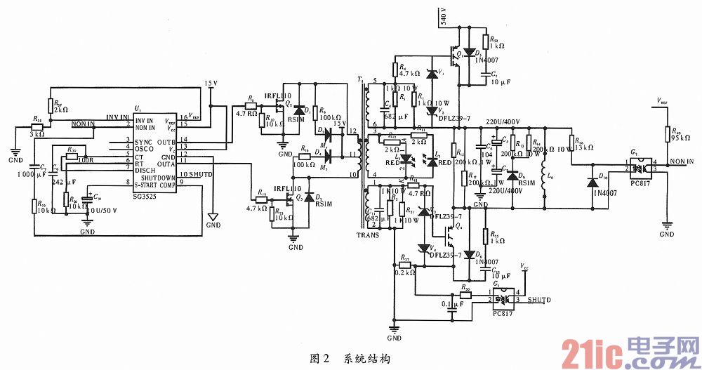
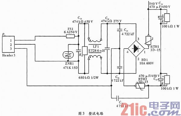
In recent years, the application of power electronic devices and PWM technology in electronic technology and power systems has become more and more mature. In this paper, the SG3525 controller is used to design the pulse power supply of the motor brake system. It is an ideal motor brake system power supply. The circuit has the characteristics of small size, convenient control, stable system and reliable performance. This article refers to the address: http:// 1 SG3525 structure and main performance The SG3525 is a current-controlled PWM pulse width modulation controller that not only adjusts the dead time by adjusting the size of the external resistor, but also functions such as soft start mode and pulse control lockout protection. By adjusting the capacitance of the CT on the 5th pin of the SG3525 and the resistance of the RT on the 6th pin, the frequency of the output control signal PWM can be changed. The voltage of the 9th pin COMP can be adjusted to change the output pulse width. The above functions can greatly improve the switching power supply. Dynamic performance and simplified control circuit design. The external circuit has a simple structure and is convenient to use, and the output driver is in the form of a pull output, which increases the driving capability. The internal contains an undervoltage lockout circuit, a soft start control circuit, and a latch. In addition, it features overcurrent protection with adjustable frequency and maximum duty cycle. Its internal structure is shown in Figure 1. The output voltage Vc of pin 13 is used as the input voltage of pin 15 of the reference voltage regulator. When Vc>8 V, the 16-pin output of the reference regulator has an amplitude of 5.1 V and an accuracy of +1%. When Vc < 8 V, the output of the reference regulator is lowered and the accuracy is also reduced. Due to the presence of an undervoltage lockout inside the chip, the undervoltage lockout outputs a high level when the undervoltage occurs on pin 15. After a NAND gate, it becomes a low level input to the bases of T1 and T5, turning off T1 and T5, the output of pin 13 is Vc, and the pulses of 11 and 14 are disabled. The control pulse output from the power drive circuit to the power FET disappears, and the converter has no voltage output, thereby achieving the purpose of undervoltage lockout protection. The base of the transistor T3 inside the SG3525 is connected to the 10 pin of the chip through a resistor. When the system has an overcurrent signal, the output of a high level is connected to the NOR gate of the output of the undervoltage lockout, resulting in 11 pin and The output of the 14-pin is forbidden for protection purposes. The soft-start function of the chip is mainly realized by the 8-pin external capacitor C3 and the transistor T3. When the system undervoltage occurs, the undervoltage lockout of the system outputs a base high to T3, which turns T3 on, and C3 starts to discharge. When the C3 voltage is set to zero, the PWM comparator outputs a high level. After passing through the PWM latch, this high level is connected to two NOR gates, which turns off T1 and T5, and 11-pin and 14-pin pulses are disabled. . When the overvoltage signal is normal, the low level of the undervoltage lockout output turns T3 off and C3 slowly charges. When C3 is charged to a high level, the PWM comparator outputs a low level, and after the PWM latch, T1 and T5 are restored to normal operation. 2 system structure design The SG3525 chip requires a small supply current of more than a dozen mA, so its power supply is supplied from a 24 V power supply through a voltage regulator chip 78M15 from 24 V to 15 V. The output frequencies of pins 11 and 14 are set for pins 5, 6, and 7. The generated two square wave signals respectively control two MOSFET tubes and are connected to the input ends of the pulse transformer. The input terminal of the pulse transformer is connected to a 15 V power supply converted from 24 V. The two outputs of the pulse transformer are connected to two IGBTs respectively, so that the 540 V DC voltage rectified by the rectifier bridge by the 380 V AC voltage is performed. Chopping, forming the rated voltage required for the motor. After the motor is powered, the brake system is loose and the motor runs; when the power is off, it is locked and the motor stops running. The system structure is shown in Figure 2. 2.1 Drive Design As shown in Figure 2, the system uses SG3525 as the main control chip. By setting the parameters of the resistors and capacitors of pins 5, 6 and 7 to control the output square wave frequency of the chip. The 11-pin and 14-pin square wave output frequencies are 1/2 of the 3-pin oscillator sawtooth. The oscillator output frequency is f, the frequency of the 11-pin and 14-output is f0 f=1/[CT(0.7RT+3RD)] (1) Fo=f/2 (2) Among them, CT, RT and RD are respectively 5-pin external capacitor C9, 6-pin external resistor R20 and resistor R39 across 5 and 7 feet. Considering the switching loss of the IGBT and the volume of the pulse transformer, select C9=2.4 nF, R20=10 kΩ, and R39=100 Ω to obtain the output frequency f0=30 kHz of the 11-pin and 14-pin. The soft-start capacitor C10 of the circuit is 4.7μF. Only when this capacitor is charged to the control chip 8 is high, the chip can work normally. Pin 11 and pin 14 form a push-pull output, and the two MOSFETs are turned on and off in sequence. When the Q2 gate is extremely high, Q2 is turned on, and Q3 is turned off. The pulse transformer has a 15 V power supply that forms a loop through the upper half of the transformer and Q2. At this time, the output of the pulse transformer produces the voltage of about 15 V at the same name of the 5 pin and the 1 pin. This voltage can drive the IGBT to turn on after filtering; when the Q2 gate is at a low level, Q2 is cut off, and the Q3 gate is extremely high. Level, Q3 is on. The intermediate contact 15 V power supply of the pulse transformer forms a loop through the lower half of the pulse transformer and Q3. At this time, the 6-pin and 2-pin of the pulse transformer output generate a voltage of about 15 V. This voltage is applied to the emitter of the IGBT, so that the IGBT can be reliably turned off. 2.2 rectifier circuit The system rectifier circuit is shown in Figure 3. After the three-phase AC power is filtered by the EMI filter inductor, the electromagnetic interference generated by the AC component is greatly reduced, and harmonic interference is also prevented. Connect a small-capacity, high-voltage, non-inductive capacitor to the EMI output to eliminate high-frequency interference. In order to increase the capacity and withstand voltage of the capacitor, connect two parallel high-voltage capacitors at the output of the rectifier bridge. The capacity of C20 and C27 should be large enough to reduce the ripple and low-frequency oscillation of the output voltage. However, C20 and C27 cannot be infinitely large. In order to meet the system output voltage ripple output requirements, this capacitor should meet In the formula, C is the filter capacitor, the unit is F; f is the rectifier circuit pulse frequency, unit Hz; U is the maximum output voltage of the rectifier circuit, unit V; I is the maximum output current of the rectifier circuit, unit A. ACv is the ripple factor and the unit is %. 2.3 BUCK circuit The motor brake system has an electromagnetic brake system at the end of the motor. When the electromagnetic brake system is powered, the brakes are separated and the motor is running. When the power is lost, the brake is braked by the spring. The excitation coil of the selected brake is rated at 190 V DC and rated at 0.55 A. The power supply of the system is AC380V AC, so it must be rectified and stepped down to ensure that the motor can run normally when the output voltage is about 190 V DC. In the system structure diagram 2, the switching transistor selected by the chopper buck circuit is an IGBT, and two IGBTs are selected, which improves the reliability of the system. The 380 V AC power supply is rectified by a three-phase silicon bridge to a 540 V DC voltage and then connected to the collector of the IGBT. The emitter is connected to the filter inductor and capacitor, and the gate is connected to the output of the pulse transformer as the IGBT drive. The load is the coil of the DC motor. The rated DC motor is rated at 190 V, so the duty cycle of the square wave signal is required. (1) Filter inductor. In this design, it must be ensured that in any case, the inductor current is continuous, the smaller the current change amount ΔI, the smaller the minimum average current, and the larger the required inductance L. At a certain ripple voltage, the output capacitance can be reduced. In engineering, usually choose △I=0.2L, the inductor size needs to be satisfied. (2) Filter capacitor. The ripple current of the inductor flows into the output filter capacitor, causing the output voltage ripple. In order to reduce the ripple of the output voltage and the low frequency oscillation of the DC voltage, the selection of the filter capacitor is particularly important. The product of the output filter capacitor and its equivalent series resistance satisfies CResr ≥ T/2, T is the switching period, and the output ripple is mainly determined by Rers. If the peak-to-peak value of the output voltage ripple is ΔUpp, the capacitance must be equal to C≥65×△I×10-6/Upp (6) 2.4 Overcurrent protection circuit The overcurrent protection loop of the system is connected to a 0.2Ω/2 W high-precision resistor on the main loop of the system for current detection. The input of this resistor is sampled and the sampling signal is input to the linear optocoupler PC817 (G1). The output of the PC817 is connected to pin 10 of the SG3525. When the system current is too large, the optocoupler PC817 LED is turned on, and outputs a high level to the SG3525's 10 pin to disable the 11-pin and 14-square wave output, so that both the pulse transformer and the IGBT stop working. The motor load coil loses power, and the brake piece locks the motor rotor under the action of the spring, thereby achieving the purpose of protection. The designed overcurrent protection circuit omits the current detecting component and the current transformer, which greatly simplifies the design circuit and isolates the strong and weak parts of the system, which better prevents interference between strong and weak electricity and enhances The reliability of the system. 2.5 regulated output loop The system's voltage regulation loop is sampled at both ends of the load coil, as shown in Figure 2. The sampling signal is input to the optocoupler PC817 (G2), and the output is passed through a voltage dividing circuit to obtain a voltage signal equal to the reference end of the SG3525, which is input to the non-inverting input of the SG3525. When the load voltage becomes larger, the brightness of the optocoupler light-emitting diode is enhanced, the optocoupler is turned on, and the current transmitted to the output terminal linearly increases. The voltage signal at the sampling point of the output decreases as the optocoupler increases. The voltage at the non-inverting input of the internal voltage comparator of the SG3525 decreases, and the output low level controls the duty cycle of the PWM so that the 11-pin and 14-pin The duty cycle of the output square wave is reduced, and the average voltage of the load coil is reduced to form a negative feedback, so that the voltage across the load coil returns to the rated value. 3 simulation results The simulation circuit is built on the simulation software Saber. The input voltage is three-phase AC380 V+5%, the output voltage is DC190 V, the output current is 0.55 A, the output power rating is 105 W, and the switching frequency is 30 kHz. The simulated waveforms of the 11-pin and 14-pin of the SG3525 are shown in Figure 4. The square wave phase difference between the 11-pin and 14-pin outputs is 180°. The two outputs directly drive the MOS tube, and then drive the IGBT through the pulse transformer. The simulation output waveform is shown in Fig. 5. The output voltage of the system tends to be stable at 190 V after a period of time, and the voltage fluctuation is small. When the actual measurement of the motor's normal operation to the brake system coil voltage, the normal operating voltage of the motor is 150 ~ 280 V, so this voltage fluctuation can be ignored, and the expected effect is achieved. At the same time, when designing the system PCB, since this system involves 380 V AC and the power supply system of the system main control chip, and the control signal part of the system is weak, it is necessary to consider the strong and weak electricity when performing PCB layout. Interference, try to place the strong power supply part on one side of the PCB board, weak power on the other side, and reduce the interference between strong and weak electricity by punching or slotting the board in the middle. In the sampling part, the optocoupler PC817 is used for signal transmission and isolation, and its layout is at the boundary of strong and weak electricity. When wiring, the power and ground wires should be widened as much as possible, and the analog ground and digital ground are also involved. The two must also be separately routed. The trace of the main control signal should also be widened to ensure accurate signal transmission. 4 Conclusion The hardware design of a switching power supply for push-pull motor brake system based on SG3525 controller is introduced. The push-pull circuit design not only overcomes the complicated problems of peripheral hardware drive, but also effectively improves the driving ability of the system and makes the system The stability is good and the output is stable. In addition, its hardware design is simple, and the layout and wiring on the printed circuit board are convenient, so it has high practical potential.
With the continuous upgrading of terminal consumption in smart city, LED lamp pole screen, as an indispensable information carrier in smart street lamp system, is welcomed by many media companies and government agencies.
LED light pole screen is mainly installed on the street light pole on both sides of the highway and the street. Because the light pole display screen has the characteristics of synchronous reception and synchronous playback, no matter how far the car goes, it is always accompanied by the HD light pole display screen. The lamp post display screen not only has unique advantages in road guidance, road condition broadcast, information release, advertisement promotion, etc., but also plays a considerable role in alleviating the fatigue of automobile drivers on the highway.
LED intelligent light pole screen can quickly get the favor of consumers, which comes from the following natural advantages:
1. It has multiple control modes of WiFi / 3G / 4G / network cable, and the Internet can update the display content of light pole screen remotely, which is simple, fast and convenient
2. The high-definition intelligent lamp pole screen adopts the best three in one technology of waterproof and UV resistant SMD in the industry.
3. The intelligent LED light pole screen presents a full outdoor high-definition and high-definition picture. It uses RGB deep gray processing to support the point by point annotation function to maintain the consistency of advertising content and color brightness. Let the color of the advertisement more gorgeous, the picture quality more high-definition exquisite.
4. The lamp pole screen body is equipped with fixed stiffener plate, which can be tensile, shockproof, self cooling, and extend the service life;
5. The high-definition intelligent lamp pole screen has the protection grade of IP65 and is not afraid of any bad weather.
Lamp Post Pole LED Screen for Advertising,Advertising Lamp Standard LED Display,Street light pole led display,Double-edged led Lamp Post Shenzhen Vision Display Technology Co,.LTD , https://www.ledvdi.com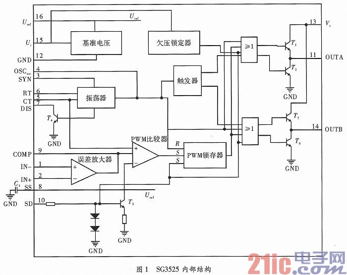
![]()

![]()
![]()