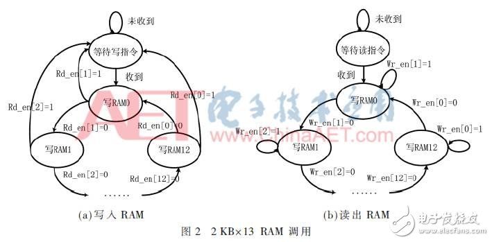
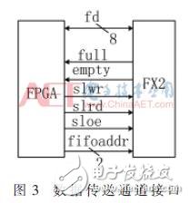
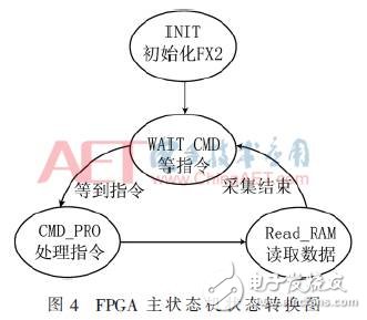
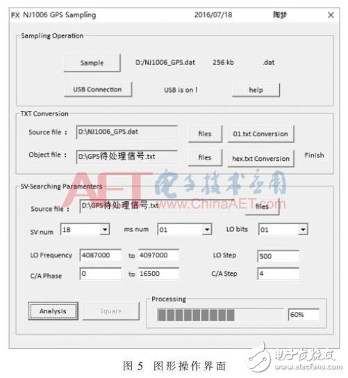
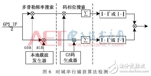
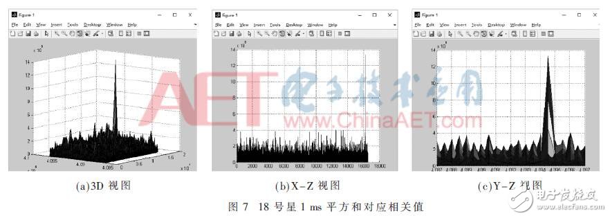
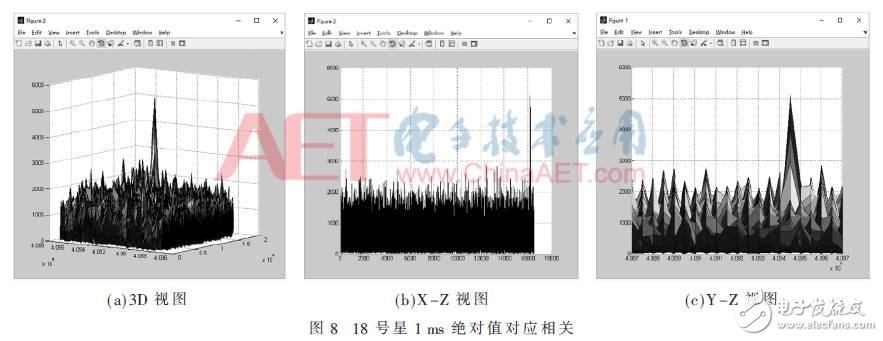
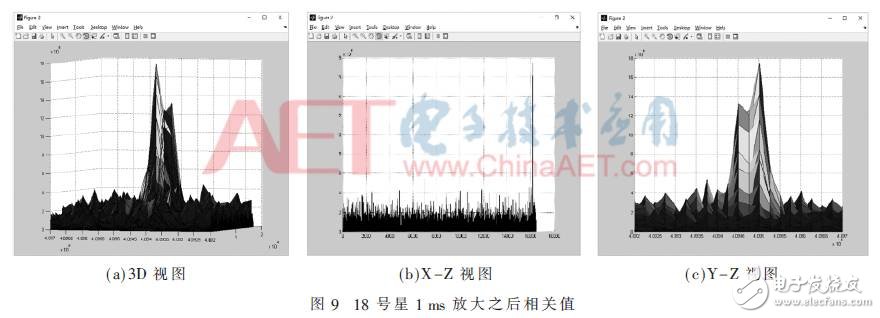
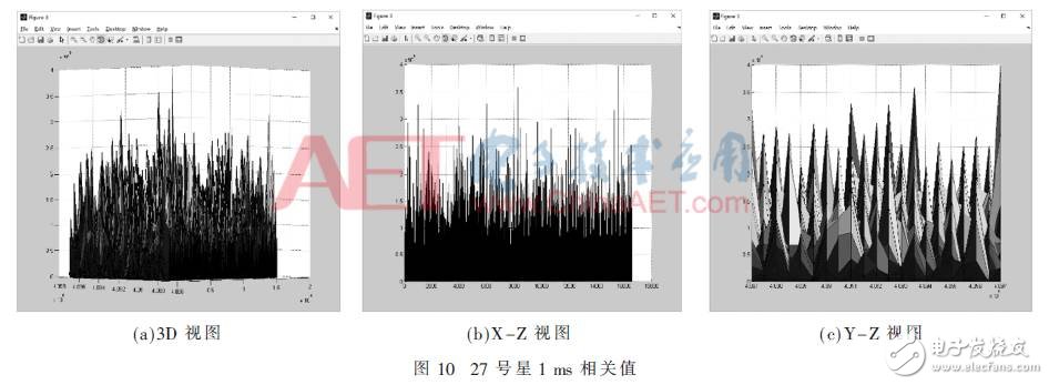
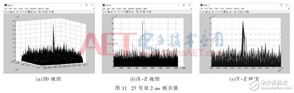
Key words: GPS IF signal; USB; signal acquisition; data analysis CLC number: TN967.1 Document identification code: A DOI: 10.16157/j.issn.0258-7998.170792 Chinese citation format: Tao Meng, Li Jincheng. GPS IF signal acquisition and analysis system design [J]. Electronic Technology Application, 2017, 43 (9): 34-38. English Reference Format: Tao Meng, Li Jincheng. Design of a system for sampling and analysis of GPS IF signal [J]. Application of Electronic Technique, 2017, 43 (9): 34-38. 0 Preface With the wide application of GPS global positioning system in providing positioning information and high-precision time information, more and more enterprises and research institutions at home and abroad are deeply researching navigation and timing chips, and to realize these functions, it is inseparable from Analysis of GPS satellite signals. Therefore, independent research and development of miniaturized, portable GPS IF signal data acquisition equipment is very important for navigation algorithm research and chip design [1]. USB interface has high data transmission rate and flexible transmission mode. It supports low speed (1.5 Mb/s), full speed (12 Mb/s) and high speed (480 Mb/s) transmission speeds, as well as interrupt transmission, control transmission, synchronous transmission and block. Four transmission modes are transmitted, and the USB interface has been widely used in the PC field [2]. The highly integrated GPS receiver RF front-end chip NJ1006 can collect GPS satellite signals in 2 bit format, and the real-time sampling rate can be reduced to about 4 MHz by bit splicing. USB2.0 transmission speed can be fully met, and from the perspective of cost and penetration, using USB2.0 is a better choice. Based on the above analysis, this paper designs a GPS IF signal acquisition and analysis system. The system uses the FPGA to byte splicing and buffering the NJ1006 digital IF signal, and uploads it to the PC through the USB interface chip (FX2 68013). A dedicated VC++ program is designed on the PC side for data reception, format conversion and analysis on the PC side. 1 system hardware and software overall architecture The overall hardware and software architecture of the GPS IF signal acquisition and analysis system in this paper is shown in Figure 1. It consists of hardware and software. The hardware part includes GPS radio receiving chip NJ1006, FPGA (cyclone EP1C12Q240C8N, with 20 060 logic units and 52 M4K memory) and USB2.0 interface chip (FX2-68013); the software part includes data receiving program, format conversion program, The data analysis program and the main control program are composed. The NJ1006 is a highly integrated GPS receiver RF front-end IC that integrates the resonant loop of the LNA and the local oscillator, reducing the number of external components and PCB area. The NJ1006 downconverts the 1 575.42 MHz GPS L1 signal, which is sampled by a 2-bit A/D converter and outputs a 2-bit digital signal (signal bit SGN and size bit MAG) with an output rate of 16.368 MHz and an intermediate frequency of 4.092 MHz to the FPGA. FX2-68013 is a USB2.0 chip introduced by Cypress Semiconductor. The chip packages various functions required by the USB peripheral interface into a simplified integrated circuit. The internal 8051 microprocessor facilitates the control and configuration of the chip [3] ]. By programming the internal 8051 of the chip, the USB2.0 chip is configured to operate in the Slave FIFO mode, and the data is transmitted asynchronously to support the high-speed data channel in FIG. 1; since the USB 2.0 chip has an I2C interface and supports external I2C memory. In order to not affect high-speed data transmission, this thesis uses FPGA to simulate an I2C memory. The host computer realizes the control of the working state of the FPGA by reading and writing the I2C memory [4]. The FPGA receives the digital intermediate frequency signal of the NJ1006, performs bit splicing and buffering, sends data to the USB2.0 chip, and uploads the collected data to the PC through the USB2.0 interface. Receive data on the PC side and perform format conversion and data analysis. The main task of the analysis is to calculate the two-dimensional correlation value of the C/A code phase and Doppler frequency of the GPS IF signal, and perform three-dimensional display by Matlab. 2 FPGA logic design 2.1 Data stitching The GPS satellite signal is received by the RF front-end NJ1006 under the 16.368 MHz clock. Since the bit width of the signal is 2 bits, and the data bus width between the FPGA and the USB is 8 bits, the serial-to-parallel conversion is required. , convert serial data to parallel data. At this point, the write data speed is reduced to the original quarter (4.092 MHz), which will greatly reduce the timing requirements required for data upload. 2.2 Data Cache The USB2.0 protocol has a fast data transfer rate, but this design uses a Windows system PC as the host computer, which is a multi-tasking system. When running, it will split multiple time slices for each application, even if only the software in this design is run. The program also cannot guarantee a stable transmission speed, which will affect the real-time transmission of data. To solve this problem, you can cache the data by adding memory. However, since the external RAM is expensive, and the data stream acquisition rate mentioned in the foregoing is about 4 MHz, and the average data transmission rate of Windows is higher than this acquisition rate, in order to ensure the continuity of the data stream, The FPGA's internal M4K memory resources can be used to generate 26 KB of RAM as a buffer. The data obtained from the bit stitching is temporarily stored in this RAM, and then transmitted to the host PC through USB2.0 for storage and analysis. In this system, the 26 KB cache space is divided into 13 2 KB RAMs, and the data obtained from the bit stitching is sequentially written into the RAM, and the cache data written with 2 KB RAM is sequentially read and transferred to the FX2, and then the FX2 is once. The 2 KB data is transferred to the host computer via USB 2.0, thereby cyclically operating the 13 memories of RAM0 to RAM12 to complete the data read and write operations. This method maximizes the use of resources and ensures real-time uninterrupted data flow. The process of writing cache data to RAM is shown in Figure 2(a). After receiving the write command of the RAM, the system first writes the collected data to RAM0. When RAM0 is full, if RAM1 is busy (ie, Rd_en[1]=1, the system reads data from RAM1), the write is terminated, the system returns to the initial state, and waits for the write command, otherwise it goes to RAM1 without interruption. data input. Thereby, the 13 memories of RAM0 to RAM12 are sequentially cyclically operated to complete the writing of data. The RAM write operation mechanism ensures real-time, uninterrupted data flow and meets data collection requirements. The process of reading the cached data is shown in Figure 2(b). After receiving the RAM read command, the system first reads the data from RAM0 and transfers it to the FX2's Slave FIFO. After the RAM0 read operation is completed, if RAM1 is in the idle state (ie, Wr_en[1]=0, the system does not write data to RAM1), the cache data in RAM1 is read without interruption, otherwise wait for RAM1 to complete the write operation. Continue reading. The 13 memories of RAM0 to RAM12 are cyclically read until the end of the acquisition. 2.3 Data Transfer Data transfer is performed by SF2's Slave FIFO mode, and the data read from the RAM is uploaded to the host PC and saved. The interface diagram of the high-speed data transfer channel is shown in Figure 3 [5]. Before starting to transfer data, configure the Slave FIFO to 2'b10 through the Slave FIFO switch address fifoaddr to enable it to write data to the FX2's Slave FIFO. After receiving the data transfer instruction, the main program monitors the empty flag of the Slave FIFO, empty and full, in real time. When the Slave FIFO is found to be not full, the data read from the RAM is transferred to the bidirectional data port fd of the Slave FIFO by controlling the write clock slwr of the Slave FIFO to form a high-speed data channel for data upload. 2.4 FPGA state transition The state transition diagram of the FPGA main state machine is shown in Figure 4. The entire state machine works at 72 MHz clock. The INIT state initializes the data of each interface of FX2, and then enters the WAIT_CMD state, waiting for the host computer to send instructions. When the host computer issues an acquisition command, the 48 B data transmission command is transmitted from the USB to the internal 8051 chip of the FX2, and then the 48 B data is written into the I2C memory by the 8051, and the first byte data [6] is analyzed. When the first byte is 8'h0a, the state machine enters the CMD_PRO state, performs instruction processing, issues a write command to the RAM to start data buffering, and then enters the READ_RAM ​​state, and after reading the signal of the empty suffix of the Slave FIFO in FX2, reads Out of RAM cache data. The RAM read and write calls are described in detail above and will not be described here. When the acquisition is over, the state machine returns to the WAIT_CMD state and waits for the next acquisition. The acquisition end mechanism in this design is divided into two cases. One is that when the data is to be written to a single RAM, the system is reading the data in the RAM, and the writing operation cannot be continued, resulting in interruption of the real-time transmission data. At this time, the host computer can not receive data for a long time, and will automatically terminate the receiving data. This is caused by the data real-time transmission data rate being higher than the upper computer receiving data rate. At this time, the software will notify the user that the data is unreliable; the other is The data received by the host computer has already met the size requirement of the collected data. At this time, the host computer actively stops receiving data, and the FX2 slave FIFO is always in the full state. The FPGA can not continue to upload data after waiting for more than the specified time, and the state machine returns to the WAIT_CMD state. The acquisition is over and waiting for the next acquisition. 3 software operation The upper computer program is written in C language MFC, and the operation interface is shown in Figure 5. The USB Connection button configures the 8051 chip in the FX2 for USB and FPGA data channel connections. Click the Sample button in the figure to issue the acquisition command. The host computer starts to call the FX2 dedicated batch endpoint upload function, repeats the loop 128 times to receive 256 KB data, waits to receive the data, and then transmits the command through the USB to synchronize the FPGA with the host computer. Work, collect data [7]. After the data acquisition is completed, the data format can be converted into ASCII code or corresponding 0-1 binary sequence through the TXT Conversion window of the software operation interface, which is convenient for the user. The parameters can be set and analyzed by the SV-Searching Paramenters window in Figure 5. The source file is the 0-1 binary sequence file after the current data acquisition and conversion, by setting the satellite number SV num (satellite 1 to 32), millisecond integral ms num (1 ms to 10 ms), quantization bit LO bits (1 bits to 10 bits) and Doppler frequency range LO Frequency, CA code phase C / A Phase and corresponding frequency step LO Step, C / A step C / A Step and other parameters, click the Analysis button, CA code And two-dimensional search of Doppler frequency. The three-dimensional data is calculated by the time domain serial capture algorithm, and the three-dimensional map is simulated by Matlab's surf function to analyze the reliability of the signal [8]. The time domain serial acquisition algorithm is shown in Figure 6. The local carrier generator selects a carrier frequency within a preset Doppler frequency range to generate two local carriers cos and sin with a phase difference of 90°. The input signal is mixed with the two local carriers to obtain an in-phase component I and a quadrature component Q. Then, the I and Q components are correlated with the locally generated C/A code sequence, and the correlation value is obtained by summing Absolute or square sum square operation by absolute value [9-10]. 4 GPS IF signal acquisition and analysis results In this paper, the satellite signal is collected, converted and analyzed through the graphical operation interface, and the self-developed miniaturized and portable GPS IF signal data acquisition device is realized. The GPS satellite signal data was collected at the ninth teaching building of Beijing Jiaotong University at 1:20 pm on January 13, 2017. At this time, the corresponding value of the 18 ms square sum operation of Fig. 18 is shown in Fig. 7. It is apparent from the figure that the frequency of the satellite is around 4.094 5 MHz and the code phase has a significant correlation peak around 16 000 points. Figure 8 is the correlation diagram of the absolute value summation of the 18th star. Comparing Figure 7 and Figure 8, it can be seen that in the case of obvious signals, both operations can find the correlation peak, but the absolute value is obtained by correlation. The value base is smaller and requires less hardware resources, compared to the squared summation of its associated peaks. Based on the full search, you can find a more accurate search after finding the relevant peak. On the basis of the full search of Figure 18, the frequency search range is reduced to 4.092~4.097 MHz, and the frequency step is reduced to 250, the CA code step is 2, and the correlation peak is amplified and analyzed. As shown in Figure 9, the method facilitates analysis of the reliability of the algorithm and signal correctness. The software also supports multi-millisecond overlays, setting the Doppler search step size, frequency, and number of CA code samples. Since the current satellite signal is weak, the 1 ms correlation value may not accurately find the correlation peak. In this case, the correlation peak can be obtained by multi-millisecond accumulation. Figure 10 shows the correlation value of the 27th star 1 ms. The correlation peak is not clearly observed from the figure, but it can be seen by the 2 ms operation in Figure 11, which is obvious at the frequency of 4.092 MHz and the code phase of 8 000. Related peaks. 5 Conclusion This paper proposes a corresponding solution for the sampling, conversion and analysis of GPS IF signals. The experiment proves that the data transmission scheme based on USB2.0 achieves the high-speed and accurate acquisition target of GPS IF signal. The GPS-based acquisition algorithm detects the reliability of the data by detecting the time domain serial acquisition algorithm in C language, which lays a solid foundation for the subsequent GPS algorithm research.
Immersion Cooling is a technique used to cool components of IT equipment that consists of submerging the computer components in a thermally conductive and dielectric liquid. Through this practice, the servers are cooled and heat is transferred from the source to the liquid.
water cooling,oil cooling,immersion cooling box,liquid immersion cooling,apw12 power supply Shenzhen YLHM Technology Co., Ltd. , https://www.ylhm-tech.com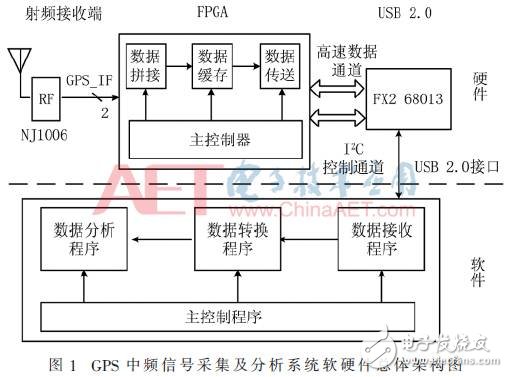
When we talk about Immersion Cooling, we also need to discuss the different types of Immersion Cooling, as well as the applications of Immersion cooling. The practice of Immersion Cooling has a multitude of benefits particularly as it allows datacenters to be managed in a greener and more sustainable manner. Environmental concerns has been a huge catalyst for the adoption of the technology in recent years.
deionized water
mineral oil
fluorocarbon-based fluids
synthetic
Immersion Cooling systems used to have a higher fluid cost than water cooling, but this is already changing.
A wide variety of liquids exist for this purpose, the most suitable being transformer oils and other electrical cooling oils. Non-purpose oils, including cooking, motor and silicone oils, have been successfully used for cooling personal computers
GPS IF signal acquisition and analysis system design knowledge sharing
Abstract: A GPS IF signal acquisition and analysis system is designed. The system uses the FPGA to serially splicing the digital GPS IF signal output from the NJ1006 RF front-end, and then uploads it to the host computer via USB, realizing the real-time high-speed between the RF front-end and the PC. Data transmission; the developed VC++ data processing program performs text conversion and data analysis on the collected GPS signals. The experiment proves that the GPS IF signal hardware and software acquisition system can not only collect GPS IF signals, but also can analyze data, and provide reliable raw data for the research of GPS baseband processing algorithms.