Solar Panel,,High Efficiency Mono Solar Panels,Bifacial Jinko Solar Panels PLIER(Suzhou) Photovoltaic Technology Co., Ltd. , https://www.pliersolar.com
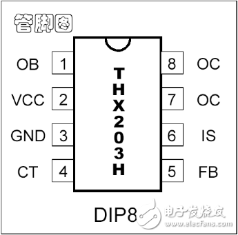
THX203H Pin Diagram
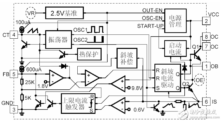
THX203H Internal Circuit Diagram
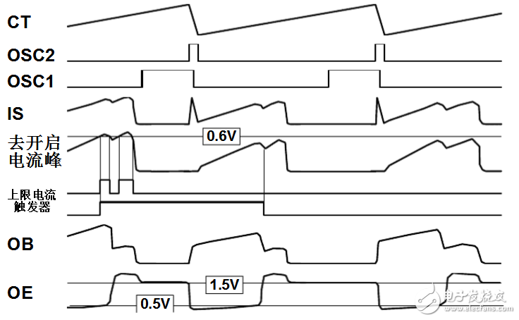
Normal Phase Switching Cycle Waveform
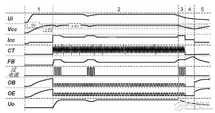
Global Waveform
Thx203h pin function and pin voltage
The THX203H is a highly integrated switching power supply controller IC designed to deliver up to 12W of continuous output power across a wide input voltage range of 85V to 265V, with a peak output power of 18W. This makes it ideal for a variety of applications requiring efficient and reliable power conversion, especially in environments where input voltage fluctuations are common.
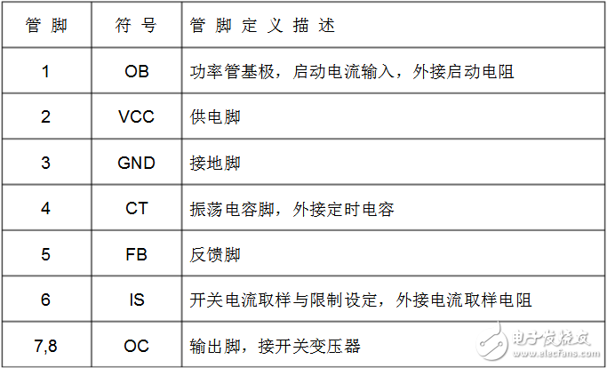
Below is a detailed breakdown of the THX203H pin configuration and internal functionality:
**THX203H Pin Diagram**
**Note:** When designing the PCB layout, ensure that there is a safe distance of at least 1mm between Pin 6 and Pin 7 to prevent electrical discharge and ensure long-term reliability.
**THX203H Pin Voltage Operation**
1. **Startup Phase:**
At power-on, the CR (current regulator) is turned off, and the FB (feedback) pull-up current source is also inactive. The OE (output enable) drives the power transistor to start charging VCC. The OB (output buffer) controls the base current of the power transistor, limiting its collector current. This ensures that the power transistor receives sufficient current to start operating safely. Once VCC reaches 8.8V, the startup phase ends, and the device enters the normal operation mode.
2. **Normal Phase:**
During normal operation, VCC should be maintained within 4.8–9.0V, and the VR provides a 2.5V reference voltage. The FB pull-up current source becomes active, and the oscillator outputs OSC1 and OSC2 control the duty cycle. If the FB voltage drops below 1.8V (typically between 1.2–1.8V), the oscillator period increases, which reduces the duty cycle and lowers the standby power consumption. If the VCC rises above 9.6V, the internal circuit compensates by feeding back to the FB, stabilizing VCC at 9.6V. This feature allows for simplified design without an external feedback loop, though the regulation accuracy may be slightly lower.
In the on-cycle, the OB provides base current to the power transistor, while OE pulls down the emitter to IS. The OB open current is a function of IS, with approximately 40mA when IS = 0V. As IS increases to 0.6V, the OB open current rises to about 120mA, effectively controlling the output current and reducing power consumption.
If the FB detects a specific current level, the device transitions into the off-cycle. During this time, the OB is pulled down, and the power transistor is not immediately turned off. Instead, OE clamps the base to 1.5V, ensuring reverse bias and improving the transistor’s voltage withstand capability. If the power transistor exceeds the upper current limit, the system triggers a protection mechanism, forcing the FB to drop and reducing the duty cycle to protect both the transistor and the transformer.
3. **Conversion Phase:**
If VCC drops below 4.3V, the oscillator turns off, and both OSC1 and OSC2 go low, keeping the power supply in an off state. If VCC continues to fall to around 3.7V, the THX203H re-enters the startup phase.
THX203H Related Article: THX203H Switch Circuit Diagram Daquan (Five THX203H Switch Circuits)
In addition to these features, the THX203H includes built-in thermal protection that increases the oscillator period when the internal temperature exceeds 140°C, preventing overheating and maintaining a maximum operating temperature of 150°C. It also features slope compensation to ensure stable operation during large duty cycles or continuous current modes. These advanced functions make the THX203H a robust and versatile choice for modern power supply designs.