Chinese Tier 1 brand Solar Panel (Longi, Jinko, Trina, Canadian, Ja etc.)
This type of product is mainly Tier 1 solar module product in China, include Longi solar panel. Jinko solar panel, Canadian Solar panel, ja solar panel etc.all of which are among the top 10 world-renowned brands. The original A grade product is mainly mono crystalline and half cut cell solar modules, with a power range of 400watts to a maximum of 700watts.quality warranty is 25 years.
A grade, this type of film is characterized by a neat and uniform appearance, printed electrode grid lines, no broken grid, no surface stains, no leakage, no aluminum package, no hidden cracks, no scratches, no black core, no reverse current, stable electrical performance, and high conversion efficiency
Chinese tier 1 brand solar panel
Tier 1 Solar Panel,Mono Solar Panel N Type,Solar Panels Bifacial 555 Watt,Solar Panel Mono Topcon Cell PLIER(Suzhou) Photovoltaic Technology Co., Ltd. , https://www.pliersolar.com
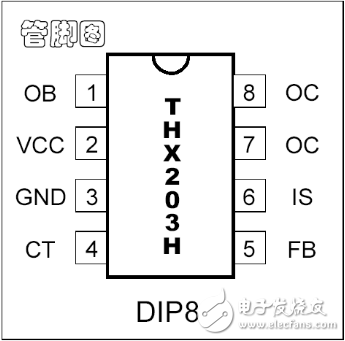
Thx203h pin diagram
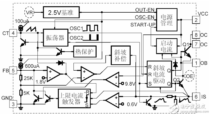
Thx203h internal circuit diagram
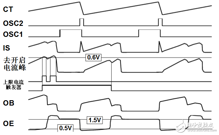
Normal phase switching cycle waveform
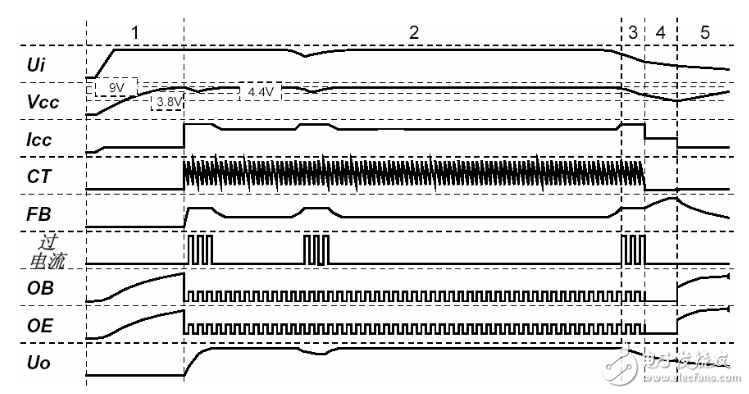
Global waveform
Using solar cell testing equipment to measure and screen, the conversion efficiency, filling factor, and appearance that meet certain standards are first level. Generally, the conversion efficiency, filling factor, and appearance of first level are better than those of level B
The level of solar panels can be divided into first level, second level, third level, and fourth level, and the first level components can be divided into first level+and first level - two levels. The second level is also the same, and the cost difference between different levels of solar panels is also very large.
TIER 1 brand include
Longi, Jinko, Trina, JA, Canadian, znshine, etc.
quality warranty
25 years
grade
original A grade (each solar panel can be checked on official website with barcode)
power range
400watt to max 700watt

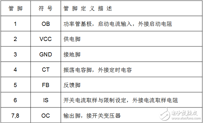
Thx203h pin function and pin voltage
The THX203H is a high-performance switching power supply controller IC capable of delivering up to 12W of continuous output power across a wide input voltage range of 85V to 265V, with a peak output power of 18W. It is designed for efficient and reliable power conversion in various applications such as LED drivers, industrial power supplies, and consumer electronics.
Below is the pin diagram of the THX203H:
Here is a more detailed pin diagram:
The following image shows the pin functions and voltages:
**Note:** When designing the PCB layout, ensure that there is a safe distance of at least 1mm between Pin 6 and Pin 7 to prevent discharge and improve reliability.
### THX203H Pin Voltage Description
1. **Startup Phase:**
At power-on, the CR (current regulator) is turned off. The FB (feedback) pull-up current source is also disabled. The OE (output enable) drives the power transistor to start charging VCC. The OB (output buffer) controls the base current of the power transistor, limiting the collector current of the power tube (ensuring the THX203H starts receiving current), which helps protect the power transistor. Once the VCC voltage reaches 8.8V, the startup phase ends, and the device transitions into the normal operating mode.
2. **Normal Phase:**
During normal operation, the VCC voltage should be maintained within 4.8V to 9.0V, and the VR output provides a 2.5V reference. The FB pull-up current source is activated. The oscillator output OSC1 determines the maximum duty cycle, while OSC2 attempts to trigger the power transistor into an open state, allowing the current peak to be controlled. If the FB voltage drops below 1.8V (typically between 1.2V and 1.8V), the oscillator period increases, resulting in a wider period until it stops. This feature reduces initial standby power consumption. If the peripheral feedback tries to increase VCC above 9.6V, the internal circuit feeds back to FB to stabilize VCC at 9.6V. This allows for output voltage regulation without an external feedback circuit, although the voltage accuracy may be slightly lower. In the on-cycle, OB provides base current to the power transistor, and OE pulls down the emitter to IS. OB's open current depends on IS, with approximately 40mA when IS = 0V. As IS increases to 0.6V, the OB open current rises to about 120mA, effectively controlling the output current and reducing power consumption. When the FB detects the specified current, the system enters the off-cycle. During the off-cycle, OB is pulled down, and the power transistor is not immediately turned off. Instead, OE clamps the voltage to 1.5V, helping the transistor withstand reverse bias and improving its breakdown voltage. If the power transistor exceeds the upper current limit, the upper current threshold is triggered first, forcing the FB to drop and reducing the duty cycle to protect both the transistor and the transformer. The upper current trigger resets at the start of the next off-cycle or when the FB voltage drops below 1.8V. Additionally, the THX203H includes built-in thermal protection that increases the oscillator period if the internal temperature exceeds 140°C, ensuring the chip temperature does not go beyond 150°C. It also features slope compensation to stabilize the on/off cycles during large duty cycles or continuous current mode.
3. **Conversion Phase:**
If the VCC voltage drops to around 4.3V, the oscillator turns off, and both OSC1 and OSC2 are set to low. The power supply remains off. When VCC further decreases to about 3.7V, the THX203H re-enters the startup phase.
Thx203h related article: thx203h switch circuit diagram Daquan (five thx203h switch circuit)