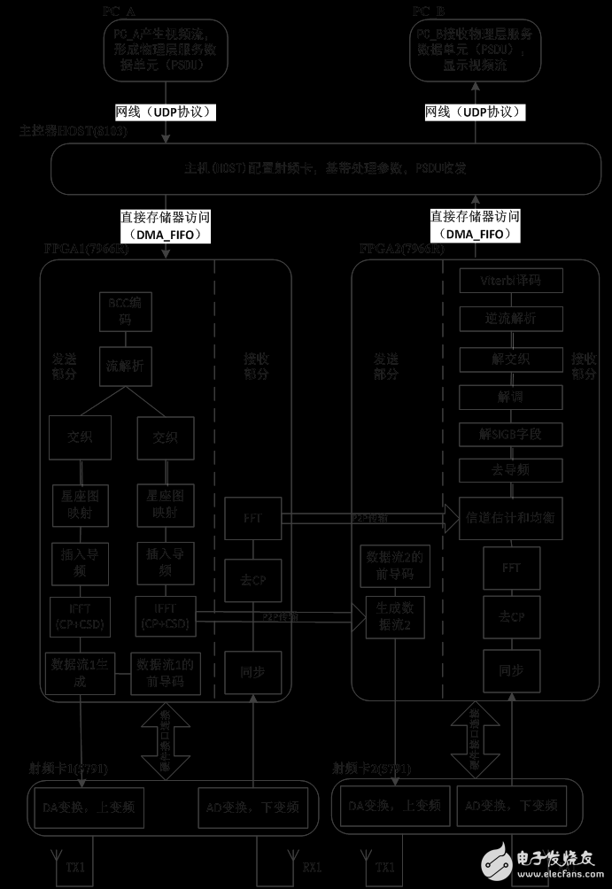
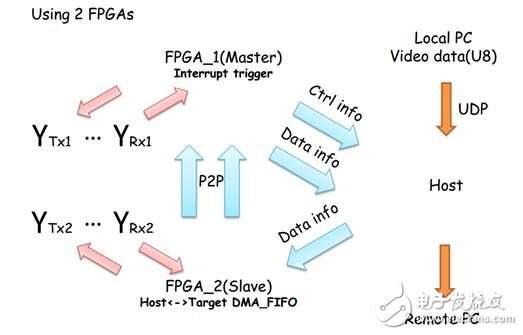
The fifth generation of mobile communication technology (5G) for 2020 is a new generation mobile communication system developed to meet the growing demand for mobile communication. According to the development law of mobile communication, 5G will have ultra-high spectrum utilization and energy efficiency, and increase the transmission rate and resource utilization by an order of magnitude or higher than 4G mobile communication, its wireless coverage performance, transmission delay, and system. Security and user experience will also be significantly improved. 5G mobile communication will be closely integrated with other wireless mobile communication technologies to form a new generation of ubiquitous mobile information network, which will meet the development needs of mobile Internet traffic increased by 1000 times in the next 10 years. 5G is no longer an air interface technology with high speed, high capability and high efficiency. It is an intelligent network that can meet different business needs and continuously improve the user experience. The integration between 5G and other wireless mobile communication technologies will be Will become an inevitable trend. Wi-Fi (wireless fidelity) technology has become one of the indispensable wireless communication technologies in daily life. In the hotspot area, the Wi-Fi and 5G convergence networking will be more effective in offloading the existing cellular network, and at the same time can greatly improve the user experience, which is one of the future development directions of 5G. The emergence of Wireless Local Area Network (WLAN) frees individuals from their homes or desks. People can connect between any two points, such as hotels, parks, shops, cafes, airports, etc., and get information anytime, anywhere. . Since the initial version of the IEEE 802.11 standard was completed in 1997, standards including 802.11b, 802.11a, and 802.11g have made WLAN applications increasingly mature and mature over the next six years. In February 2007, the IEEE 802.11n 2.0 draft determined that this new standard was developed across the ages, with breakthroughs in transmission rates that can reach 300 Mbps (20 MHz channel) or even 600 Mbps (40). Under the MHz channel). In response to the explosive growth in traffic demand and the provision of good backward compatibility, IEEE 802.11ac, which is considered by the industry to be the fifth-generation Wi-Fi, is on the horizon. Two project teams (Task Group, TG) have been set up within the IEEE to target the Very High Throughput (VHT). Two projects are proposed for future wireless network applications. IEEE 802.11 Ac and IEEE 802.11ad. In January 2014, the draft 802.11ac was officially adopted. The IEEE 802.11ac protocol has a physical layer transmission rate of up to 6933.3 Mb/s under eight spatial streams, 256QAM modulation, 5/6 code rate, 160 MHz transmission bandwidth, and 400 ns guard interval. As a continuation of the 802.11n standard, 802.11ac has been greatly improved on the basis of the original. In addition to using critical OFDM, MIMO, and space-time coding, 802.11ac also introduces multi-user multiple-input multiple-output (MU-MIMO) technology that allows for higher-order modulation— - 256-QAM doubles the transmission rate. In addition, 802.11ac expands the channel bandwidth to 40MHz, 80MHz, or even 160MHz based on 802.11n's 20MHz (optional 40MHz) channel. The frame structure of the physical layer adds a VHT_SIG_B area to describe the data length to be transmitted, the modulation scheme and coding strategy (ModulaTIon and Coding Scheme, MCS), and the single-user/multi-user mode. Of course, meeting the above requirements also faces greater challenges from complex technologies. 802.11ac can provide high-speed transmission rate, good user experience, etc., but due to the complexity of its mechanism, the difficulty of system hardware implementation is increased. At present, 802.11ac devices are not many in the market. This paper studies the ultra-high-speed WLAN system based on IEEE 802.11ac, and uses its NI-PXI platform to develop and verify its prototype, which is a new generation of Wi-Fi technology and 5G technology. Research is of great significance. This paper aims to implement a system prototype based on the IEEE802.11ac standard on the NI-PXI platform. The parameter specifications for the system design are as follows: 3.1 Overview The project needs to reach a data transmission rate of hundreds of megabytes, thus requiring high-speed data processing. In hardware implementation, we have chosen to use high-performance FPGAs to achieve high-speed requirements. However, developing such a system requires us to be very good. Master the VHDL or Verilog HDL language. At the same time, the project also involves RF, which is also a huge difficulty for us. We only want to focus on the baseband design of the 802.11ac protocol. NI LabVIEW software and its hardware platform are for us. A gospel solves all our worries, allowing us to focus on what we want to focus on, greatly shortening our development cycle. In the following, we will describe the NI-based 802.11ac ultra-high-speed wireless LAN prototype. 3.2 Hardware platform The hardware design of the prototype is based on the NI-PXI platform. The hardware diagram is shown in the figure below. Two FPGA boards are connected to the RF adapter in the chassis. The platform mainly includes the chassis, controller, and FPGA. Module, RF transceiver module four parts, the performance and main functions of each module are as follows: Figure 1 System hardware platform physical map (1) NI PXIe-1082 chassis: The chassis contains 4 hybrid slots, 3 PXI Express slots, 1 PXI Express system timing slot, up to 1 GB/s dedicated bandwidth per slot and 7 GB /s system bandwidth, compatible with PXI, PXI Express, CompactPCI, and CompactPCI Express modules. The chassis provides power, cooling, and PCI and PCI Express communication buses for the controller and modules, as well as a range of I/O module slot types and integrated peripherals. (2) NI PXIe-8115 controller: This system uses NI PXI-8115 as the controller, located in the leftmost slot of the chassis. It is a high-performance embedded controller based on the Intel Core i5-2510E processor for PXI systems. It has 2.5 GHz baseband, 3.1 GHz (single-core Turbo Boost mode) dual-core processor and single-channel 1333 MHz DDR3 memory. It is equipped with standard equipment such as Ethernet and serial port. It can choose its own operating system. This design uses Windows system. (3) NI PXIe-7966R: For the data transmission of wireless LAN, the data processing capability is mainly considered, and the FlexRIO module is selected. It consists of two main components: an FPGA module and a FlexRIO adapter module that provides high-performance analog and digital I/O. These can all be configured by the LabVIEW FPGA software. The FPGA module uses the NI PXIe-7966R, which includes a Virtex-5 SX95T FPGA and 512 MB of onboard DDR2 dual-port RAM. This FPGA contains 640 DSP slices, which can be used for signal processing, digital filtering, FFT logic, etc. In addition, the theoretical throughput of the onboard dual port RAM is 3.2GB/s. The PXIe-7966R supports high performance P2P streaming. The FPGA module in this system mainly implements the baseband data processing of the transmitting end and the receiving end. (4) NI 5791 RF Adapter: The NI 5791 is an RF transceiver with continuous frequency coverage from 200 MHz to 4.4 GHz, with both the TX and RX terminals having an instantaneous bandwidth of 100 MHz. It features a single-stage steering architecture that provides ultra-high bandwidth in the compact form factor of the NI FlexRIO Adapter Module. The onboard synthesizer (local oscillator) is used to set the center frequency of the acquisition and generation and can be exported to other modules for Multiple Input Multiple Output (MIMO) synchronization. Users have direct access to the raw ADC and DAC data of the NI FlexRIO FPGA Module. In addition, the NI FlexRIO FPGA Module and PXI platform provide a method for synchronizing ADC and DAC data necessary to implement channel expansion. 3.3 System Design In such a real-time high-speed transmission system, system architecture design is particularly important. Good architecture design is the premise of correct operation of the system and the key to improve system performance. The structural framework of the prototype system is shown in Figure 2. The system design is mainly divided into three parts: PC end design, HOST end design and FPGA end design. The PC end design is based on C# language to realize video codec and so on. The HOST end and FPGA end design are mainly based on LabVIEW programming. The former Responsible for parameter configuration, data transmission, etc., the latter is responsible for implementing the physical layer module of the IEEE 802.11ac protocol. Data synchronization is also required between the three. The design of each part will be described in detail below. Figure 2 Overall architecture of the system 3.3.1 Physical layer data communication prototype physical layer data communication is mainly carried out between PC, HOST and FPGA, and its flow direction is shown in Figure 3. The system sends two channels of data stream, so two FPGAs are needed to generate data and interface with the transmitting RF antenna. In order to complete the transmission of wireless data, the system architecture is also equipped with a data transmission user Local_PC and a data receiving user Remote_PC. In addition, a controller Host is used as an intermediate carrier to develop a LabVIEW algorithm for data baseband transceiving processing. Assume that the transmitted data is a video stream. First, the transmitting local_PC encapsulates the video stream data into a U8 format and packs it. The FPGA1 generates an interrupt to request data from the Host. After the Host obtains the interrupt request, it generates a new interrupt to the Local_PC to request the encapsulated data. Local_PC waits for an interrupt request to arrive, that is, sends a U8 packet to the Host. After the Host obtains the U8 data, it responds to the interrupt of FPGA1 and sends data to FPGA2 through the DMA_FIFO. FPGA2 completes the operation of each module in the baseband processing process of the transmitting end to form two data streams. One of the data streams is transmitted to FPGA1 through the P2P mechanism. The two channels of data are sent to the RF card through the hardware interface, and the RF stream is processed by the RF card in the RF card and sent through the transmitting antenna; the received signal is transmitted to the two FPGAs through the RF card, and the data in the FPGA 2 is transmitted through the P2P. To FPGA1, the subsequent baseband receiving process is completed in FPGA1, and the processed bit stream is transmitted back to the Host through the DMA_FIFO, and the Host transmits the data to the Remote_PC, and displays the video stream in the Remote_PC. Figure 3 prototype physical layer data flow diagram 3.3.2 HOST Design In this system design, the HOST terminal is an important link between PC, FPGA and RF card. Its main work is: b. Complete the transfer of baseband parameters and the establishment of DMA_FIFO. The baseband parameters to be considered are: modulation mode, length of each frame, and length of each block of Viterbi. Two DMA_FIFOs are established: the bit stream on the HOST side is passed to the FPGA (HOST to Target), and the bit stream decoded on the FPGA side is passed to the HOST (Target to HOST). c. Complete the transmission of RF parameters, including bandwidth selection, carrier frequency selection, DC offset repair parameters, transmit power value, and amplifier gain settings. d. It is also necessary to complete the data transmission and synchronization configuration between the two FPGA boards. This part is discussed in detail in the FPGA design. e. Complete the automatic gain control (AGC) and adaptive modulation (AMC) function modules. The following discusses in detail the implementation of the main functional modules on the HOST side. The HOST settings are as follows: The sending PC sets the local IP address to the return address 192.168.1.7, the destination IP address to the actual address of HOST, and the destination device port number to 12270. In addition, you need to set a port number to receive the data request interrupt sent by HOST, set it to 2000; the receiving PC sets the local IP address and the remote device IP address as the actual address, and then defines a port number for receiving remote data. 12271. This allows Socket data to be sent and transmitted using Socket sockets. (2) Adaptive modulation (AMC) scheme Although high-order modulation and high coding rate can improve the spectral efficiency, this imposes strict requirements on the signal-to-noise ratio parameter of the communication system. If the noise energy reaches a certain level, the system will be caused. As the bit error rate increases, the bit error performance is greatly reduced, thereby reducing the throughput of the system. In order to ensure the effective throughput performance of the system, when the signal to noise ratio is low, the low-order modulation mode and the coding rate should be selected. When the signal-to-noise ratio is high, the high-order modulation mode and the coding rate can be selected. Therefore, the design adopts adaptive modulation (AMC) technology to ensure the transmission quality of the link by adjusting the modulation mode and coding rate of the wireless link transmission with constant transmission power. The process of implementing AMC requires stable signal power, which requires the introduction of automatic gain control (AGC) techniques to ensure signal energy stability. During the operation of the AGC, the initialization power p0 allows the RF amplifier to obtain an initial amplification factor. For the receiving end, an expected energy pref needs to be set to determine the energy of the signal when the AGC process tends to stabilize. During the communication process, when the channel environment changes, the energy pr of the received signal will change continuously, and the adjusted power parameter pd will also change (pd is a negative parameter used to control the RF amplification factor). When the received signal energy is reduced, the RF amplifier of the receiving antenna increases the amplification factor. When the received signal energy increases, the RF amplifier of the receiving antenna reduces the amplification factor, so that the signal energy is maintained near the expected energy pref. At the beginning of the communication process, the adjustment power parameter pd can be arbitrarily set. The adjusted power parameter pd (logarithmic form) in the AGC process satisfies the formula (1), where pd_new is the updated value of pd. Consider a single-user MIMO2 & TImes; 2 system using BCC channel coding. The fixed BCC coding rate is 1/2. A simple AMC setup scheme is shown in the following table. The interval in the table is the NI-PXI platform using NI- A set of reference intervals for the 5791 RF Adaptation Module to test. The corresponding expected energy pref = -8dBm. Table 1 Relationship between AMC modulation mode and adjusted power parameter pd Pd interval (dB Select modulation method (-27, -18) BPSK (-18,-12) QPSK (-12,-8) 16QAM (-8,-5.5) 64QAM (-5.5,-4) 256QAM
Description
-Press the button, power on; release it, power off
Features
A push button switch is a switch that has a knob that you push to open or close the contacts. In some pushbutton switches, you push the switch once to open the contacts and then push again to close the contacts. In other words, each time you push the switch, the contacts alternate between opened and closed. These types are commonly called latching switches. There are also Non latching push button switches that only maintain the switch contacts when the switch is help in position. Once the switch is let go, the current is broken and the switch turns off. Push switches are usually a simple on-off switch.
Push Light Switch,Mini Push Button Switch,Push Button Switch Types,Push Button On Off Switch Ningbo Jialin Electronics Co.,Ltd , https://www.donghai-switch.com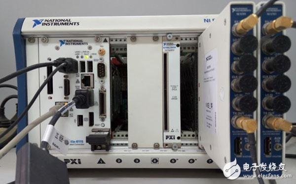
1) The system is based on the IEEE 802.11ac protocol;
2) The system operates in the 2.4 GHz/5 GHz band;
3) The system is configured with 2 transmit antennas and 2 receive antennas;
4) The transmission bandwidth of the system reaches 20MHz;
5) Modulation optional mode: BPSK, QPSK, 16QAM, 64QAM, 256QAM, and adaptive modulation according to the received signal to noise ratio;
6) System spectrum efficiency: up to 10 bit/s/Hz (in 64QAM mapping mode, the code rate is '5/6');
7) The demodulated receiving constellation map can be displayed;
8) High quality transmission of video can be achieved.
The physical layer content of the IEEE 802.11ac protocol that the prototype needs to implement is:
1) Transmitter: BCC coding, stream analysis, modulation, insertion of pilot, CP, IFFT;
2) Receiver: synchronization, de-CP, FFT, channel estimation and equalization, de-pilot, demodulation, counter-current analysis, Viterbi decoding. 
a. Complete the sending and receiving of the PC-side video stream. This part uses the UDP protocol through the network cable. In this respect, LabVIEW has a mature design, calling and configuring the IP address, packet length parameters, and so on. For the received data, taking into account the tail biting operation of Viterbi design, the data packet must be zero-padded, and the design is completed by array conversion, etc., and the bit stream sent to the PC end needs to be tail-tailed.
(1) Video stream transceiver configuration
The communication between the PC and the HOST is done through the UDP protocol. UDP has the characteristics of simple connection and fast speed. As long as the sender PC, the NI-PXI master controller and the receiver PC are all connected in the same LAN, UDP can be used to realize high-speed data communication.
-Contact resistance:≤5Omohm
-Switch Function: S. P. D. T. with lamp.
-Various shapes and colors: yellow, blue, red, black, green
Design of Next Generation Ultra-High Speed ​​Wireless LAN Prototype System Based on NI-PXI
1 Introduction