Today's consumers and original equipment manufacturers (OEMs) demand high quality and high reliability as the basic requirements of automotive products. It is estimated that in-vehicle electronic components are growing at a compound annual growth rate of 8.1% (CAAGR) [1], and this development will drive continued growth in demand for zero-defect products. The challenge for semiconductor suppliers is to meet this requirement while introducing low-cost products. In this article, we will focus on best practices for achieving zero defects in small-scale trial production of semiconductor products to the formal production stage. In the early stages of the product life cycle, due to the latest products, the probability of launching components with the potential risk of early failure is highest. This article refers to the address: http:// Figure 1 "bathtub" shape curve shows the semiconductor failure rate as a function of time Figure 1 shows a typical "bathtub" shape curve showing the reliability of a new product as a function of time without starting any production with any best practices. Early failures are seen as time zero/low mileage failures. After a series of corrections and reliability improvements, this failure rate can be reduced over time to a random failure rate (if all system problems are resolved). As the failure rate drops to a random level and the product is aging, the in-vehicle electronics begin to reach their expected service life, resulting in an increased failure rate due to component aging. In general, the dominant failure mechanism in one phase is not necessarily the same as the dominant mechanism in other phases of the product life cycle. Using some well-known best practices, this zero-defect approach focuses on the "early lifespan" portion of the curve. Some of the main methods used for zero defect placement of products include adequate quality inspection (TFQ) range, dedicated build process factors (eg, new technology for burn-in), and implementation of outlier control. Successful implementation of real-time data and device analysis and tiered approach enables early detection of failures, accelerated situational awareness, and timely failure-correction measures without impacting users. The first way to achieve zero defects during product launch is to apply TFQ best practices. These best practices include VMIN and VMAX based on device temperature characteristics and extreme process condition tolerance (cornerlotevaluation); special functional tests for device design; and other best practices such as turn-off leak testing. A key aspect of TFQ is to set the correct test limits based on statistical data. In addition, you must ensure that all device design structures that cannot be tested in the final package are wafer tested. A good example of oxide integrity stress testing of large capacitor structures is if the test and design layout allows direct access to the capacitor itself. Other good test implementation practices include those that focus on ensuring more than 95% of high test coverage, high gate count device scan implementation, overvoltage stress testing, and statistical quiescent current testing. In summary, these methods can ensure that outlier components are screened out from a large number of products while meeting product specifications. In order to maximize the overload test value: 1) all components that fail in the overload test should be submitted for comprehensive electronic and physical failure analysis; 2) find the root cause of each fault feature; 3) implement the correct Corrective action. Corrective measures typically include: reducing defects from the wafer fabrication process technology itself, improving automated test equipment stress testing to improve the efficiency of the fault detection mechanism, and implementing improved outlier control upstream of the process to increase the results of the overload test to 100% yield. . Figure 2 shows the improved over-load test yield obtained after performing test enhancements based on what was learned during the gradual mass production phase. Figure 2 shows the change of yield over time after the overload test, and the improvement of the yield after the implementation of the test improvement. It is important to note that tools, equipment, and manpower are required for overload testing, so this is an expensive screening method from an investment perspective. If the root cause and correction method of the fault are clear, and there is a large degree of confidence that the result can reach the target level, then the overload test may be used or not used. Finally, to achieve the goal of zero defects during the time to market, extensive outlier control best practices need to be implemented. As the level of automation, data collection, and data transfer continue to increase, so does the opportunity to enhance control and real-time feedback in the process of enhancing outlier control. Outlier control includes statistical box limit (SBL), statistical yield limit (SYA), dynamic parameter outlier control (DPO), or component average test (PAT). At the wafer test level, methods for reducing defects include some post-test outlier control techniques such as composite wafer charts, single die screening, and composite wafer charts and edge strips. Figure 3a depicts a test screening method for eight wafers surrounding the test "single die"; Figure 3b depicts another form of "single die" position test screening method. Figure 4 shows an example plot of final test yield (before overload test) and points that do not meet statistical yield limits. This point is an outlier, a risk point that requires further screening and analysis, and a non-conforming product may also appear. People's expectations for the automotive industry are zero defects. Using the best practices described above, the desire to deliver zero defects and protect consumers is achieved, and through the necessary learning process, we have a quicker grasp of ways to reduce defects. Many of the challenges in reaching a zero-defect goal are daunting and not necessarily successful. That's why quality inspection best practices, special processes (such as overload testing, etc.) are used, and outlier control best practices will enable semiconductor suppliers to meet unprecedented demands for true safety products.
1. Display, touch screen, PC system integration slim design
2. Using the projected capacitive screen, supports 10 point touch, handwriting and multi-point gesture;;
3. Pure flat , Aluminum alloy + sheet metal structure ;
4. Flexible configuration, with many options of different RAM/SSD/HDD, supports OS of Android/windows/Linux etc.
5. High safety; Stable performance:
6. Simple installation for embedded/desktop/wall mounting
All In One Pc,All In One Computer,Touch Screen Aio Pc,All In One Touch Pc Guangzhou TouchWo Electronics Co.,Ltd. , https://www.touchaio.com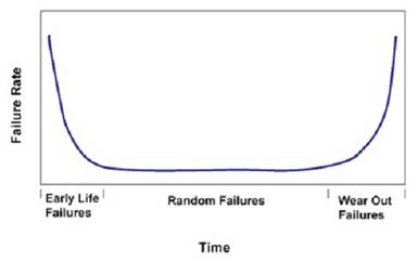
The second method used to screen early failures is to build a specialized build process based on technical risks. An example of such a special process is the implementation of an overload test during gradual mass production. In general, overload testing should be implemented in response to new technologies and user-customized designs that have potential risks that miss unknown defects. In order to use this method correctly, you need to understand the process technology and design associated with critical component access and selected conditions for overload testing (voltage, temperature, and stress duration). When properly implemented, the overload test speeds up better in-line detection and defect screening for early failures, facilitating an earlier understanding of failures in the product life cycle and taking a series of fault corrections without giving Users have an adverse effect. 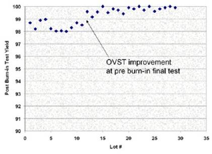
Figure 3 depicts some examples of pattern outlier screening methods for rejecting outlier components in wafer level testing, which can be done using automated test equipment and image recognition software. In Figure 3a, the die marked with a question mark was considered unacceptable in the wafer test because the eight chips around it were identified as unacceptable in the wafer test and thus implicated. In Figure 3b, the die marked with a question mark is also implicated by a list of failed chips. These techniques for detecting outliers are also often referred to as "single die" methods. 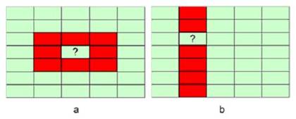
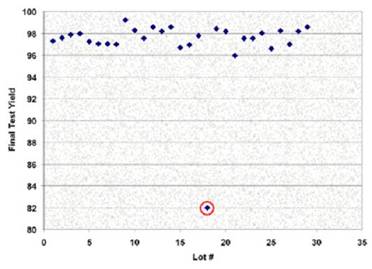
Figure 4 shows an example of a statistical outlier screening method. A color block marked with an orange circle indicates that the statistical yield limit was not reached in the final test. At this time, the point should be marked out and the engineering analysis should be used to find out the cause of the abnormal yield drop. After the failure analysis and root cause investigation, it was found that the deployment of this point is most likely to lead to the occurrence of non-conforming products. As a starting point for step-by-step production, the initial limits should be set according to the same or similar design or technique until more data can be collected to set the statistics-based limits. With the gradual mass production of the product, if sufficient statistical test data has been collected and analyzed, the SYL and SBL limits can be set according to the specific test device. Thereafter, over time, the SYL and SBL limits can be adjusted periodically to ensure that the limit is always valid during the screening of outliers.