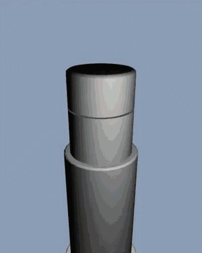
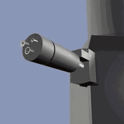
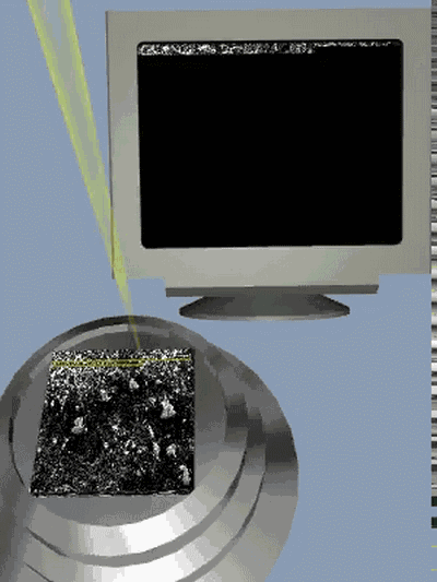
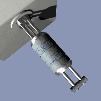
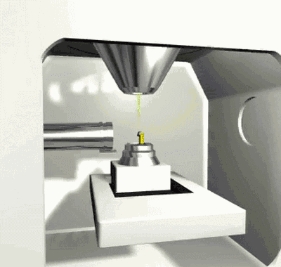
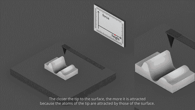
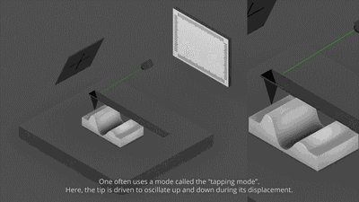
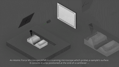
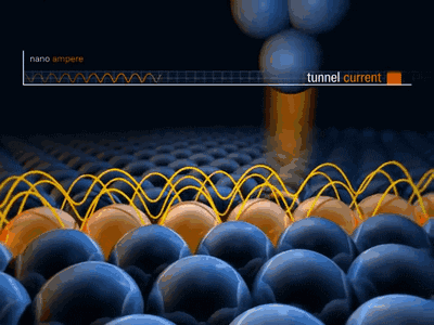
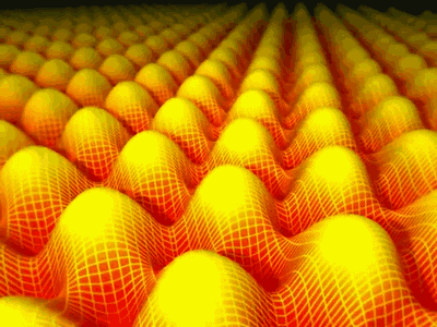
The microscopic analysis of the material can obtain the organizational structure of the material, reveal the basic properties and basic laws of the material, and occupy an important part in the material testing technology. For all kinds of microscopic analysis equipment such as SEM, TEM, AFM, STM, etc., every member of the material will certainly be unfamiliar. Recently, Xiao Bian discovered some electron microscopy animations and was shocked. The original boring electron microscopes can become so vivid that they have less gossip, and the following will share with everyone. Scanning electron microscope (SEM) Scanning electron microscope imaging uses fine-focus high-energy electron beams to excite various physical signals on the sample surface, such as secondary electrons, backscattered electrons, etc., and these signals are detected by corresponding detectors. The intensity of the signal is consistent with the surface morphology of the sample. The corresponding relationship, therefore, can be converted into a video signal to modulate the brightness of the picture tube to obtain the image of the surface topography of the sample. SEM work map The part of the energy (30-50 eV) lost due to the inelastic scattering of the valence electrons of the incident electrons and the valence electrons in the sample excites the nucleus out of the nucleus. The energy is greater than the valence electrons of the work function that escapes from the sample surface into a vacuum. Free electrons, this is secondary electrons. Electron emission map Secondary electron detection map The surface state of the secondary electron sample is very sensitive and can effectively display the microscopic appearance of the sample surface with a resolution of 5 to 10 nm. Secondary electron scanning imaging The incident electrons are reflected close to the nucleus where there is no energy loss; they include both elastic backscattered electrons formed by interaction with the nucleus, and non-elastic backscattered electrons formed by interaction with the sample nucleus. Backscattered electron detection map When the back-reflected signal is used for topography analysis, its resolution is much lower than that of secondary electrons. The relative size of the atomic number of the corresponding region can be discriminated based on the degree of lightness or darkness of the backscattered electron image, whereby the composition of the metal and its alloy microstructure can be analyzed. EBSD imaging process Transmission electron microscope (TEM) Transmission electron microscopy (TEM) projects an accelerated and focused electron beam onto a very thin sample. The electrons collide with atoms in the sample and change direction, resulting in solid-angle scattering. The size of the scattering angle is related to the density and thickness of the sample. Therefore, different shaded images can be formed, and the image will be displayed on the imaging device after being enlarged and focused. TEM work diagram TEM imaging process STEM imaging is different from TEM of parallel electron beams. It is accomplished by scanning the sample with focused electron beams. The difference from SEM is that the detector is placed under the sample and the detector receives transmitted electron beams or elastically scattered electrons. The beam, after amplification, shows a bright field image and a dark field image on the screen. STEM analysis diagram The incident electron beam irradiates the surface of the specimen with elastic scattering. The energy value lost by a part of the electrons is the characteristic value of an element in the sample. Thus, the energy loss spectrum (EELS) is obtained, and the element composition and chemical bond of the thin specimen microdomain can be obtained by using the EELS. And electronic structures, etc. are analyzed. EELS schematic Atomic Force Microscopy (AFM) A micro-cantilever that is extremely sensitive to weak forces is fixed at one end and has a tiny tip at the other end. Because there is a very weak force between the atom at the tip of the tip and the atoms on the surface of the sample, the force is controlled through the constant The micro-cantilever will fluctuate perpendicular to the surface of the sample. The micro-cantilever is measured to correspond to the position change of each point of the scan, so that information on the surface topography of the sample can be obtained. AFM principle: interaction between needle tip and surface atoms The scanning mode of the AFM has a contact mode and a non-contact mode. The contact type uses the change of the repulsive force between the atoms to generate the sample surface profile; the non-contact type utilizes the change of the attractive force between the atoms to generate the sample surface profile. Contact mode Dynamic mode Scanning Tunneling Microscope (STM) The intensity of the tunnel current has an exponential dependence on the distance between the tip and the sample. According to the change of the tunnel current, we can get small fluctuation information on the sample surface. If the xy direction is scanned at the same time, the three-dimensional sample surface shape can be directly obtained. This is the working principle of the scanning tunneling microscope. Probe The tunnel current is extremely sensitive to the distance between the tip and the sample surface. The distance decreases by 0.1 nm and the tunneling current increases by an order of magnitude. Tunnel current When the needle tip scans on the surface of the sample, even if the surface has only an atomic-scale fluctuation, it will be displayed through the tunnel current. Then, the computer will use the measurement software and data processing software to process the information into a three-dimensional image to be displayed on the screen. STM scan imaging Monoatomic manipulation: Atomic-level patterns can be obtained by using a probe to lift a single atom off the surface and move away from the surface, move laterally to a predetermined position, and release atoms from the probe back onto the surface. Moving Atomic Mapping Wireless Ccd Barcode Scanner,1D Ccd Barcode Scanner,Scanning Qr Code On Screen,Qr Code Screen Reader Guangzhou Winson Information Technology Co., Ltd. , https://www.barcodescanner-2d.com