Design of all-electric anti-skid brake controller for racing car based on CPLD/DSP
1 Introduction
The racing brake system is a relatively independent subsystem on the racing system. It is used to withstand the static weight of the car, dynamic impact loads and kinetic energy when absorbing the brakes of the car to achieve braking and control of the car. Its performance directly affects the car's rapid response, safe braking and survivability, which in turn affects the overall performance of the car. This paper designs the hardware and software of the all-electric anti-skid brake controller of the racing car, and finally studies the control law suitable for the racing brake.
2 system hardware circuit design
The racing brake controller consists of an anti-skid controller and a motor drive controller. Both controllers are based on DSP chips. The anti-skid controller is mainly controlled by the slip rate, and outputs a given brake pressure. The DSP chip is used as the CPU, plus the racing wheel and the wheel speed signal conditioning circuit. The motor drive controller mainly adjusts the brake pressure and controls the motor current. It also uses the DSP chip as the CPU, plus the peripheral circuit motor current feedback conditioning circuit, overcurrent protection circuit, brake pressure conditioning circuit, and four sets of three-phase full bridge. The inverter circuit and the like constitute a motor drive controller.
2.1 DSP's minimum system
The DSP's minimum system mainly involves memory expansion, JTAG interface configuration, reset circuit, ADC module settings, and clock circuit design.
1. Off-chip memory expansion. The off-chip memory is to compensate for the lack of internal DSP RAM, and it is also convenient to download the program to the off-chip high-speed StaTIc RAM during the debugging process. The external static random access memory uses CY7C1041CV33. The DSP can use either on-chip program memory or off-chip program memory, as determined by the pin XMP knife MC. JTAG interface. When the program needs to be debugged, the program download is completed through the JTAG interface, which is connected to the parallel port of the PC through the emulator.
2. Reset circuit and clock source module. A low-level reset circuit that generates a power-on reset and a manual reset with a RC circuit generates a reset signal. In addition to a hardware watchdog, its output generates a reset signal WDRST. The two inputs of the power chip are both +5V, and the output is +1.9V and +3.3V power supply for the DSP. The output power supply has two reset signals respectively. When the power supply is unstable or too low, a reset signal will be generated.
3. Hardware configuration of the analog-to-digital conversion ADC module. The analog-to-digital conversion ADC output voltage is 2V, requiring the output to be terminated with a low ESR capacitor of 10μF to the analog ground. If the software is set to external reference mode, ADCREFP can be connected to an external input with a 2V reference voltage and a low ESR capacity of 1μF to 10μF. Otherwise, the accuracy of the AD's internal reference source will be affected.
2.2 Racing front wheel and brake wheel speed signal processing circuit
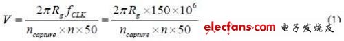
The anti-skid controller is mainly controlled by the slip ratio to prevent the car from slipping. The pressure reference value is adjusted by the deviation of the slip ratio to track the given slip rate. The anti-skid controller must have a conditioning circuit for the front wheel and brake wheel speed signals, mainly to obtain the feedback slip rate. The racing speed signal is replaced by a free-rolling front wheel speed signal. The speed sensor is installed on the front wheel and the brake wheel of the car. When the wheel rotates, the speed sensor generates an AC signal in the form of a sine wave. Each time the wheel rotates, the speed sensor emits a 50-cycle sinusoidal AC signal. The amplitude of the sinusoidal AC signal varies with the speed of the wheel. The signal is a sine wave signal with a bias voltage of 2.5V, a peak of 0.3V, and a maximum signal amplitude of no more than 5V. The sine wave signal is converted into a square wave of the same frequency and sent to the capture unit of the DSP, and the count value interval ncapture of the adjacent rising edge of the square wave is captured, and the rotational speed value V of the wheel can be calculated. Since the CPUCLK is 150MHz, the capture time base is one of the timers, n is the division factor of the CPUCLK, and the radius of the wheel is the calculation formula of the wheel speed:
6 layer PCB Board is, in general, a4 Layer PCB Boardwith 2 extra signal layers added between the planes. The 6-layer PCB classic stackup includes 4 routing layers (2 outer layers + 2 internal layers) and 2 internal planes (one for ground and the other for power). This enhances the EMI dramatically by offering 2 buried layers for high-speed signals and 2 surface layers for routing low-speed signals. The signal layers should be closed to the adjacent planes.
6 Layer PCB Stackup and Design
What is PCB stack UP?
PCB Stack up refers to the arrangement of copper and insulation layers that make up PCB before the layout design of circuit board. Although stacking allows you to get more circuits on a single board through various PCB layers, the structure of PCB stacking design has many other advantages:
The PCB layer stack can help you minimize circuit noise and radiation and reduce impedance and crosstalk problems in high-speed PCB layouts.
A good stacked PCB stack can also help you balance the need for low-cost, efficient manufacturing methods and focus on signal integrity issues.
Proper PCB stacking can enhance the electromagnetic compatibility of your design.
For PCB-based applications, stacked PCB configurations are usually good for you.
Why do PCBs stack up?
The irreversible development of modern electronic products has increasingly pushed PCB towards such needs as miniaturization, light weight, high speed, better functionality and reliability, and longer life, which has led to the popularity of multi-layer PCB. Two or more Single Sided PCB and/or Double Sided PCB are stacked together by a combination of semi-solid adhesives called "prepregs" to form multilayer PCBs through reliable predefined interconnections between them. There are three or more conductive layers in a Multilayer PCB , two of which are outside, and one is synthesized in an insulating board. With the increasing complexity and density of PCB, some problems may arise, such as noise.
One of the most important factors to determine the performance of product electromagnetic compatibility (EMC) is to plan the optimal multi-layer stack up. The carefully designed cascade can minimize radiation and prevent the circuit from being disturbed by external noise sources. Good stacked PCB substrates can also reduce signal crosstalk and impedance mismatch. However, poorer stacking may increase EMI radiation, because impedance mismatch will lead to reflection and ringing in the system, which will greatly reduce the performance and reliability of the product. Then, this article will focus on the layer stack definition, design rules and basic considerations.
Most six-layer PCB consist of four signal routing layers and two planes. From an EMC perspective, a 6-layer Printed Circuit Board is usually better than a 4 Layer PCB board.
6 Layer PCB stackup
6 layer 1.6 MM standard stackup and thickness
One stack-up NOT to use on a six-layer PCB board is the one shown in Figure 1. The planes provide no shielding for the signal layers, and two of the signal layers (1 and 6) are not adjacent to a plane. The only time this arrangement works even moderately well is if all the high frequency signals are routed on layers 2 and 5 and only very low frequency signals, or better yet no signals at all (just mounting pads), are routed on layers 1 and 6. If used, any unused area on layers 1 and 6 should be provided with "ground fill" and tied into the primary ground plane, with vias, at as many locations as possible.
Fig. 1 One of the stackup methods of 6-layer PCB
This configuration satisfies only one of our original objectives.
With six layers available the principle of providing two buried layers for high-speed signals is easily implemented as shown in Fig. 2. This configuration also provides two surface layers for routing low speed signals.
Fig. 2 Less common 6 layer PCB stackup
This is a probably the most common 6 layer PCB stack-up and can be very effective in controlling emissions, if done correctly. This configuration satisfies objectives 1, 2, & 4 but not objectives 3 & 5. Its main drawback is the separation of the power and ground planes. Due to this separation there is no significant interplane capacitance between power and ground Therefore, the decoupling must be designed very carefully to account for this fact.
Not nearly as common, but a good performing stack-up for a six-layer PCB is shown in Fig. 2.
Fig. 3 Another performing six-layer PCB board stackup
H1 indicates the horizontal routing layer for signal 1, and V1 indicates the vertical routing layer for signal 1. H2 and V2 represent the same for signal 2. This configuration has the advantage that orthogonal routed signals always reference the same plane. The disadvantage is that the signals on layer one and six are not shielded. Therefore the signal layers should be placed very close to their adjacent planes, and the desired board thickness made up by the use of a thicker center core. Typical spacing for a 0.060" thick board might be 0.005"/0.005"/0.040"/0.005"/0.005". This configuration satisfies objectives 1 and 2, but not 3, 4, or 5.
Another excellent performing six-layer PCB board stackup is shown in Fig. 4. It provides two buried signal layers and adjacent power and ground planes and satisfies all five objectives. The big disadvantage, however, is that it only has two routing layers -- so it is not often used.
Fig. 4 Another excellent performing six-layer PCB board stackup
It is easier to achieve good EMC performance with a six-layer circuit board than with a four-layer circuit board. We also have the advantage of four signal routing layers instead of being limited to just two. As was the case for 4 layer PCB boards, it is possible to satisfy four of our five objectives with a six-layer PCB. All five objectives can be satisfied if we limit ourselves to only two signal routing layers. The configurations of Figures 2, 3, and 4 all can all be made to perform very well from an EMC point of view.
6 Layer PCB Stackup for EMI/EMC
EMI/EMC Return Current 6 Layer PCB Issue
EMI/EMC Return Current 6 Layer PCB Solved
Types of 6 PCB stack up-how to choose?
PCB materials and stackup thickness commonly used in multilayer circuit boards.
6
Layer Stackup - 2.0mm thickness (non-preferred materials but possible)
layer order
layer name
material type
material description
dielectric constant
thickness
copper weight
1
top
copper
signal
0.035mm
1 oz
2116+7628
prepreg
4.7+4.7
0.12mm+0.185mm
2
inner 1
copper
plane
1 oz
core
4.6
0.6mm
3
inner 2
copper
plane
1 oz
2116
prepreg
4.7
0.12mm
4
inner 3
copper
plane
1 oz
core
4.6
0.6mm
5
inner 4
copper
plane
1 oz
2116+7628
prepreg
4.7+4.7
0.12mm+0.185mm
6
bottom
copper
signal
0.035mm
1 oz
Final board
thickness: 2.0mm±0.2mm
6 Layer PCB Quote and Price
We provide the lowest price and fast turnover of 6-layer PCB real-time quotation service. For on-demand pricing and ordering of your next printed circuit board project, please contact online customer support or send us your documents (GERBER, etc.)for quick quotation.
6 L ayer PCB Prototype Price
We are a trustworthy and reputable PCB manufacturer in China. We have affordable prices on the 6-layer PCB Prototype . We can provide customers with 6-layer PCB board in accordance with RoHS standard. With laminated material, it can match the high temperature in the assembly process.
Of course, at the same time, we also provide sample production services for other PCB products to verify your design as soon as possible.
With regard to delivery, we can provide 24-hour, 72-hour urgent service. No matter where you are in the world.
We have abundant experience in manufacturing multi-layer circuit boards, not only in the production process, but also have many years of professional PCB engineers.So if you have multilayer PCB to produce, no matter how many layers, just let us know.
What size of 6-layer circuit boards can you produce?
According to our PCB manufacturing capability, we have no size limitation.
PCB Laminate Types
We offer a variety of PCB laminates ranging from FR4 130Tg for lower heating temperatures up to FR4 180Tg for higher temperatures. Also offered are Polyimide, Taconic, Rogers and Nelco material types.
Manufacturable Thickness of 6-Layer Circuit Board
As with the number of PCB layers we can manufacture, we still have no restrictions on the thickness of the six-layer PCB and can manufacture it.
PCB Surface Finish Types
We offer various PCB finishes including HASL (Solder), ENIG, Immersion Silver, Immersion Tin, Hard Gold, Entek/OSP, Unclad, Pb Free HASL, Selective Gold and ENEPIG.
Why order 6 layer PCB from JHY PCB?
You will get it after check below advantages.
1. Good quality and price: We are experienced in producing six layer PCB, cost and time can be controlled well. This can help our customer to order good boards in cost-effective price.
2. Short Turnaround Times:
3. No Minimum Quantity: 1 pcs of PCB can be offered.