The figure is the principle circuit of the OTL field output stage. Like the normal audio OTL circuit, it uses the two transistors V2 and V3 to supply the positive and negative portions of the scanning current iYV required for the deflection coil. The prescribed positive direction of iYV is the direction flowing into the deflection yoke in this figure. During the (t1 to t2) half cycle in which V2 is turned on, its current i2 flows into the coil through the DC blocking capacitor C to form the positive half of iYV. At this time, V3 is cut off, and i3=0. Capacitor C is charged by i2. When t=t2, iYV=0. During the half cycle of (t2~t3), V3 is turned on, V2 is turned off, the charge on the capacitor C is discharged through V3 and the coil, and the current i3 constitutes the negative half of iYV. The DC voltage at point D is ECC/2. V2 and V3 work in Class B or Class A and B. The place where they are handed over corresponds to the scanning forward center iYV=0. If the two tubes are not well connected or the magnification difference is large, the waveform of iYV at the junction is not a straight line, and the pattern at the center of the screen is distorted. Therefore, some feedback components need to be added in the actual circuit to make the output waveforms of the two tubes symmetrical. This article refers to the address: http:// The input voltage Uin is from the previous field push stage. The polarity of the V1 collector and emitter voltage waveforms is opposite. During the period from t1 to t2, the voltage at point A is higher than the on-voltage of the V2 tube, so V2 is turned on. The voltage at point B is lower than the on-voltage of the V3 tube, so V3 is off. In the period from t2 to t3, on the contrary, V3 is turned on and V2 is turned off. Therefore, the V1 tube plays the role of dividing an input signal into two excitation signals (both V2 and V3 for exciting push-pull operation). The (output) signal at point D, fed back to the input of V1, improves the waveform and also stabilizes the DC operating point.
Yuhai Company is engaged to research
and development of piezoelectric products
and related piezoelectric products, the related piezoelectric products includes the piezo sensors and transducer.
The Ultrasonic Transducer is a kind of transducer that converts the ultrasonic signal into electric signal, or vice versa. Ultrasound transmitter and receiver is a transducer that can transmit and receive ultrasound. Ultrasound sensor is a kind of sensor, in essence, it is also a transmitter and receiver. The working principle of this kind of equipment is similar to that of radar and sonar. Active ultrasonic sensors can emit and receive reflected waves, and determine the distance of the target by measuring the time interval between transmission and reception. Passive Ultrasonic Sensor is actually a microphone that can convert ultrasonic signal into electrical signal.
Ultrasonic Sensor Ultrasonic Sensor,Piezo Sensor,Ultrasonic Piezo Disc,Ultrasonic Piezo Elements Zibo Yuhai Electronic Ceramic Co., Ltd. , http://www.yhpiezo.com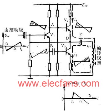
The induced voltage pulse of the reverse path (see Figure 8-37, but in the opposite direction, because the direction of iYV is opposite) is applied to both V2 and V3 tubes. For the off-state tube (for example, V3 in the reverse time of Tt/2 after t1), the direction of this pulse voltage is the direction of the power supply voltage (the power supply of the V3 tube is the DC voltage ECC/2 of the capacitor C). Conversely, its amplitude ULM is given by (8-15) and is very large. When it exceeds ECC/2, the V3 tube is subjected to a negative voltage. Therefore, the power supply ECC of the OTL field output stage is usually high to avoid this. For a conducting tube (such as V2), the reverse pulse voltage ULM is superimposed on the tube with the power supply ECC/2, during which the current of the tube is close to IPP/2, so the power consumption is relatively large.
During the forward conduction period, since the current linearly decreases from IPP/2 to zero, and the ULM does not exist, the power consumption is relatively reduced. Since the direction of the UL is different for the two tubes V2 and V3, the power consumption of the V2 is larger than that of the V3. This is the difference between the field scanning OTL circuit and the ordinary audio power amplification OTL circuit. The withstand voltage requirements of the V2 and V3 tubes are also much higher than those in the conventional OTL, which is also a feature of the field scan OTL circuit. The current tolerance ICM of the V2 and V3 tubes is at least larger than IPP/2, and the specific value is related to the deflection power index RI2PP and the R of the deflection yoke. Therefore, the transistors used in the field scanning OTL output stage are high-power low-frequency amplifier tubes. Their linearity and two-tube symmetry are also considered. Feedback circuits are usually added to improve the waveform of the sweep current and reduce the requirements for the V2 and V3 tubes.
According to the working principle and materials used, the ultrasonic transducer has Piezoelectric Transducer, electrostatic transducer (capacitive transducer), magnetostrictive transducer, electromagnetic acoustic transducer, mechanical transducer and other types [1].