Introduction At present, due to the simple structure and low sampling rate of the recording and playback chip, the sound quality in the embedded system is relatively poor, which can not meet the requirements of people for high-end living and learning embedded systems. If the sound card technology can be applied to the embedded system , the sound quality of the whole system will rise to a new level due to the powerful function of the sound card. Through analysis, WSS (Windows Sound System) compatible sound card and PC ISA bus interface principle, we apply the sound chip CS4235 to the DSP-based embedded system. The sound chip is not used in the existing sound card because it is more flexible and convenient to design, and can be added or deleted according to the needs of the system; the DSP is not used in the MCS51 series because the system requires too much system resources for the sound card operation, MCS51 This capability is not available, otherwise the hardware interface circuitry will be quite complex.
Our LED products have 5 year warranty.
We are the best supplier for your light-emitting diode.
We
supply variety of 400Nm LED products. Including Through-hole 400nm LED ,
SMD 400Nm LED and high-power 400nm LED. We can also produce 400nm LED
according to your requirement.
For the Through-hole Light Emitting Diode 400nm LED,
we
can customize the shape, the lighting angle, the number of emitting
source, the flat pin LED and braided LED. Such as: 5mm purple 400nm LED,
5mm purple 405nm LED, 5mm purple 410nm LED, 5mm purple 415nm LED, 5mm
purple 420nm LED, 5mm purple 425nm LED, 5mm purple 430nm LED. 3mm Purple 410nm LED, 3mm Purple 415nm LED, 3mm Purple 420nm LED, 3mm Purple 425nm
led, 3mm Purple 430nm led, 3mm Purple 400nm LED, 3mm Purple 405nm LED, 3mm Round Purple LED ect.
There are many other shapes for your choose. Customized purple LED are available
For the SMD LED 400nm LED,
we
can supply dual-chip purple LED, three-chip purple LED, multi-chip
purple LED, high voltage LED, flashing purple LED and variety of size
SMD LED. For instance: 3528 SMD purple 400nm LED, 3528 SMD purple 405nm
LED, 3528 SMD purple 410nm LED, 3528 SMD purple 415nm led, 3528SMD
purple 420nm led, 3528 SMD purple 425nm LED, 3528 SMD purple 430nm LED. 2835 SMD Purple 400nm LED, 2835 SMD Purple 405nm LED, 2835 SMD
Purple 410nm LED, 2835SMD Purple 400nm LED, 2835SMD Purple 415nm LED,
2835SMD Purple 420nm LED, 2835SMD Purple 425nm LED, 2835SMD Purple 430nm
LED.
There are also have many other shapes to choose, like the
5050 SMD Purple LED, the 5730 SMD Purple LED ect. You can choose any one
of them for your requirement.
365nm LED is a ultraviolet LED. Common ultraviolet LEDs are like: ultraviolet 400nm LED, ultraviolet 405nm
LED, ultraviolet 410nm led, ultraviolet 415nm led, ultraviolet 420nm LED, ultraviolet 425nm
LED, ultraviolet 430nm LED and so on.
400nm LED 400Nm LED,SMD 400Nm LED,Waterproof 400Nm LED,400Nm 1W LED Shenzhen Best LED Opto-electronic Co.,Ltd , https://www.bestsmd.com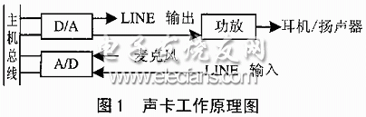
1 CS4235 Principle and Structure 1.1 Sound Card Working Principle 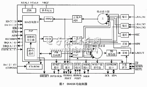
Figure 1 shows the basic working principle of the sound card: the host sends the digitized sound signal to the digital-to-analog converter (D/A) via the bus, and converts the digital signal into an analog audio signal; The digital converter (A/D) converts the input signal of the microphone or CD into a digital signal and sends it to a computer for various processing.
1.2 CS4235 Functional Structure WSS is an audio subsystem standard defined by Microsoft Corporation for the unified sound card standard and finally provides multimedia extensions for Windows applications, including hardware platform and software interface [1]. CS4235 is a sound card core chip that adapts to WSS and provides ISA bus interface. Except for sound collection and playback, all other controls depend on the host; it takes up more host time, but the cost is relatively low. The functional block diagram of the CS4235 is shown in Figure 2. As can be seen in Figure 2, the CS4235 is a complete audio subsystem IC that provides 16-bit stereo ADCs and DACs, on-chip reconfigurable digital filters, analog gain and attenuation values ​​for analog and digital mixers. Optional serial interface, full-duplex channel with simultaneous recording and playback capabilities. The documentation for CS4235 is described in reference [2].
Due to space limitations, the analog hardware part of CS4235 is not introduced here, but the digital hardware interface problem between CS4235 and DSP is mainly studied. Because TMS320F206 (referred to as F206) is a low-cost, high-performance 16-bit fixed-point arithmetic digital signal processor (DSP), cost-effective, has become an ideal substitute for high-end microcontrollers, in communications, voice processing, military, instrumentation Instruments, image processing and other fields have been widely used [3], so the system uses F206 as DSP. The 8-bit parallel interface provided by the CS4235 is compatible with the ISA bus. Is it also compatible with the DSP's external expansion bus? The signal pins and simple descriptions of the CS4235 and ISA bus interfaces are listed in Table 1, and the corresponding pins of F206 are also listed accordingly. As can be seen from Table 1, to achieve direct DSP operation on the CS4235, the DSP system must provide the above ISA bus signals. DSP chips generally provide data signal lines, address signal lines, I/O read/write signal lines, and READY signal lines. They also have multiple interrupt input pins. However, they do not directly have DMA function pins. This gives DSP and CS4235. The interface between the two brings inconvenience, which is the main problem to be solved in this article. Table 1 Signal pin signal pin of CS4235 and ISA bus interface Brief description DSP (F206) corresponding pin SD<7:0> Bidirectional system data bus D<7:0> SA<11:0> System address bus A< 11:0> IOR I/O read command is decoded by IS and RD. IQW=IS+WR IOW I/O write command No AEN address enable signal READY IOCHRDY I/O channel is ready for INT2 (actual application, just Select 1 interrupt line to connect to DSP) IRQ interrupt request signal: IRQA=IRQ5, IRQB=IRQ7 IRQC=IRQ9, IRQC=IRQ11, IRQD=IRQ11 IRQE=IRQ12, IRQF=IRQ15, IRQG=IRQ10 No DRQ DMA request signal: DRQA=DRQ0 DRQB=DRQ1 DRQC=DRQ3 No DACK DMA response signal: DACKA=DACK0 DACK1=DAC, DACKC=DACK3 RS RESET Sound card reset signal 2 DSP and CS4235 hardware interface 2.1 F206 DDR operation using direct memory access F206 The key to the function is that the chip provides two signal pins: HOLD/INT1 and the HOLD operation of these two signals is controlled as follows. 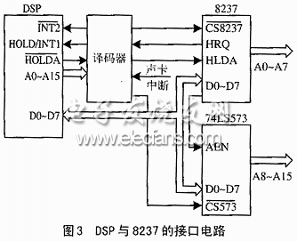
1 . An external device can drive this pin low to request control of the external bus. This will trigger an interrupt if the HOLD/INT1 interrupt line is enabled. 2. In response to an interrupt, the software logic can cause the processor to signal an acknowledge that it will relinquish control of its external bus. According to the external address signal (A15"A0), the data signal (D15"D0), and the memory control signal () are placed in a high impedance state.
As can be seen from 1, 2, the F206 HOLD operation allows direct memory access to external programs, data, and I/O space, but this function is implemented in the INT1 interrupt routine, thus the interrupt line INT1 is falling and rising. It should be sensitive along both. When F206 detects a falling edge, it completes the current instruction being executed and then forces program control to go to the interrupt service routine, which executes the IDLE instruction. According to IDLE, it becomes active and the external bus is placed in a high impedance state. Only after detecting a rising edge on the HOLD/INT1 pin, the CPU exits the IDLE state, becomes inactive, and returns the external bus to the normal state.
From the above analysis, it can be seen that the difference between the DMA operation of the F206 and the DMA operation in the PC. In the PC, after receiving the DMA request signal, the CPU forces the CPU to tristate its address, data and some control pins after the end of the current bus cycle, thereby giving control of the bus and giving one. DMA response signal; after the DMA operation is completed and the DMA request signal is invalid, the CPU resumes control of the system bus. In C2XX, the DMA request signal will cause the F206 interrupt, and the software command will be issued in the interrupt program to make the F206 signal pins tri-stated, and also give a DMA response signal; after the DMA operation is completed, but the F206 detects After the DMA request signal is invalid, although the bus returns to the normal state, the F206 is still in the interrupt routine. From the above analysis, although the interrupt needs to protect the breakpoint and the scene, the processing speed of the F206 DMA is much lower than that of the PC. After all, the F206 also implements the DMA operation, so that the DMA controller 8237 can be used to implement the sound card. DMA operation access. 2.2 DSP and DMA controller 8237 interface circuit 8237 is a high-performance programmable DMA controller chip, which can be easily connected to the CPU to achieve direct data exchange between external devices and memory. Its internal structure and pin signals can be found in [4]. The controller is programmed to provide multiple types of control features to optimize system performance and increase data throughput with data rates up to 1.6 MB/s. Figure 3 shows the main circuit of the F206 and 8237 interface, in which 8237 is sent to the DSP to request the control bus DMA request signal HRQ, which is decoded by GAL16V8 and sent to the HOLD/INT1 pin of the DSP; 
The DSP DMA response signal is also sent back to the 8237 HLDA pin via GAL16V8 decoding. The role of address latch 74LS573 is to latch 8237 the high 8-bit address A8"15 output through data line D0"7 during the DMA service cycle. Since the DSP does not directly provide the sum, and signals, these signals can only be decoded by the GAL16V8.
The circuit shown in Figure 3 provides four channels of peripherals requesting DMA service signals, and the 8237 directly has the AEN pin, which satisfies all the requirements in Table 1, so that the interface between the DSP and the sound card can be correctly implemented. In actual work, we set the 8237 DREQ1 and DACK1 as the sound card's playback channel according to the sound card's usage in the PC. The 8237's DREQ3 and DACK3 are the sound card's acquisition channels. The sound card's interrupt request signal IRQ7 is reversed by GAL16V8 and DSP. Pin connection. 2.3 System working principle and timing The DMA operation process of the DSP system shown in Figure 3 can be described by Figure 4, and the working sequence is shown in Figure 5. The working principle and operation sequence of the system will be described as follows with reference to Fig. 4 and Fig. 5: 1 CS4235 sends DMA request signal DREQ to DMA controller 8237; 2 8237 sends bus request signal HRQ to DSP; 3 DSP pin detects lower jump edge After entering the INT1 interrupt, after the protection of the breakpoint and the scene, the IDLE instruction is issued, the DSP pin level becomes low, and the external DMA request is responded; 4 8237 takes over the bus, first sends a DMA request response signal DACK to the CS4235, indicating Allow CS4235 to perform DMA transfer, and then send the address and read/write commands in sequence according to the initial address set and the number of bytes to be transferred, so that data is directly exchanged between RAM CS4235 until all data exchange is completed; 
After the 5DMA transfer ends, the bus request signal HRQ to the CPU is automatically cancelled. At this time, the DSP detects the rising edge of the pin, and the DSP returns to the next instruction of the IDLE instruction. The DSP obtains the control of the bus and continues to execute the program in INT1.
Build the Best 400nm UV LED !


