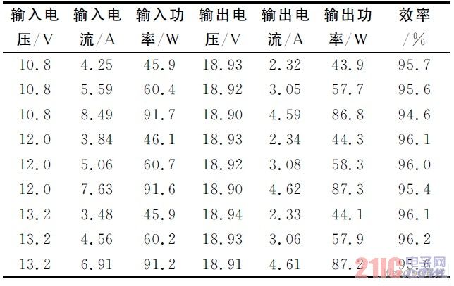
0 Preface This article refers to the address: http:// The rapid development of the information society has made people increasingly dependent on laptops, hoping to get information anytime, anywhere, but the use of laptops is always unsatisfactory. With the car power supply, users are not worried about their computers being unable to work due to insufficient power, whether on the road or in the wild. At present, many on-board power supplies on the market are to raise the 12 V voltage of the car battery to AC 220 V, and then supply power to the notebook through the adapter of the computer itself. However, the two voltage conversions lead to a decrease in efficiency, and the power of the car battery is quickly used up, resulting in abnormal operation of other electric devices on the vehicle. This design converts the 12 V DC power output from the car cigarette lighter directly into a 19 V voltage that can be used by most notebook models. The adjustable range is ±0.5 V. The input voltage ranges from 10 V to 15 V. Even if the input voltage has large fluctuations, the output voltage has a good adjustment capability. 1 How the boost converter works The car's cigarette lighter outputs a DC voltage of 12 V, which does not exceed 13.8 V even when the engine is running, which is lower than the 19 V voltage normally required for notebook computers. The voltage converter is converted by a boost converter. The basic circuit is shown in Figure 1. It consists of a power switch T, a diode D, a storage inductor L, and a filter capacitor C. The inductor is continuously charged and discharged, and the induced voltage is applied to the power supply voltage to generate an output voltage higher than that provided by the car cigarette lighter. The boost converter circuit can be viewed as being controlled by two switches, a power switch S and a diode D. Only one of the switches is allowed to close at any given time. The two operating states of the circuit are shown in Figure 2. (1) S is turned on, and D is turned off: the input DC power source UIN forms an IIN current path through the inductor L and the switch S. The DC power supply charges the inductor, the current of the inductor L increases linearly, and the electrical energy is stored in the coil in the form of magnetic energy. At this time, the diode D is reverse biased, and the output load current IOUT is supplied by the energy originally stored on the capacitor C, as shown in Fig. 2(a). (2) S cutoff, when D is turned on: Since the current in the inductor L cannot jump, a reverse polarity induced voltage as shown in Fig. 2(b) is induced in the coil. Therefore, the polarity of the induced voltage is left negative right positive. At this time, the diode D enters the forward conduction state, and the energy stored in the inductor during the S conduction period is supplied to the capacitor C and the load RL through the diode D. C The energy charged at this stage is supplied to the load RL during the next S cutoff period. Let the power switch S have a duty cycle of D1 and the diode D has a duty cycle of D2. Since only one switch is turned on at any time, then: 2 PWM control The power switch S in the boost converter is implemented with a power MOSFET that operates in the switching state, see Figure 2. After a series of pulses are applied to the gate, the power tube will be constantly in an alternate state of switching, and the ratio of the on-off time can be changed to adjust the output voltage. Suppose a period is t, t = tON, the positive pulse of the pulse width modulation pulse is sent to the gate of the power tube, K is turned on; when t = tOFF, the modulation pulse sent to the K tube becomes zero volt or Negative bias, S is in the off state. Waveform (3) shows the ripple current of the inductor, increasing the size of the coil reduces ripple, but it also increases the physical size of the device. The coil should not be too small, otherwise it will not be able to provide enough energy when the MOSFET is turned off, which will make the adjustment of the output voltage worse. The coil used in this design is 56 μH. All control functions are completed by the catalyst chip UC3843 produced by Unitrode. It has functions such as feedback voltage comparison, error amplification, pulse width modulation, overcurrent protection and undervoltage protection [4]. The chip generates a pulse width modulation signal for the power tube, and controls the on/off of the switch tube and adjusts the output voltage by detecting the output voltage and current signals. The input and output voltages are smoothed by a series of low-power capacitors. The main circuit is shown in Figure 4. The four large-capacity electrolytic capacitors (C1 to C4) connected in parallel at the input end function as a power supply filter, and C5 is used to filter out high-frequency harmonic components generated when the circuit operates. Coil L1 is connected in parallel by several different lengths of enameled wire to reduce the effect of the surface on high speed switching. The high-power switching element K1 uses IR's IRL2505. The source/drain resistance of this device is only 8 mΩ during operation, so the power consumption is very low. Schottky diode D1 is packaged in TO220 with a maximum operating voltage of 45 V and a forward voltage drop of 0. The current at 63 V is 16 A. Low ESR electrolytic capacitors C6 to C9 are used to smooth the output voltage and reduce the ripple voltage. Capacitor C10 is used for high frequency decoupling. The output voltage is divided by R1, R2, R3 and P1 and fed to the voltage feedback input of IC1. The clock frequency of the IC is determined by the RC networks R8 and C13 and operates at approximately 42 kHz. A power supply decoupling circuit consisting of R12, C15, and C16 to ensure the reliability of IC1 operation. 3 test See Table 1 for the power and efficiency of the power adapter during normal operation. Its high efficiency (usually 95%) not only reduces the load on the car's battery, it also reduces the power consumption inside the adapter. The PCB size is smaller than the notebook's own power adapter. Figure 4 schematic diagram of the main circuit Table 1 Test results and efficiency This paper presents a 12 V DC/19 V DC solution for on-board power supplies that uses automotive batteries to provide continuous power to laptops. The program can not only meet the needs of ordinary users when they travel by themselves, but also enable industry users such as roads, industry and commerce, tax audits, public security and geology to ensure the power supply of laptops at any time, and fully utilize the wireless office characteristics of laptops. . 12V UPS Charger, Restorer and Tester 3-in-1 Recovery system , is fit for 12V/36 Ah~300Ah lead-acid battery banks, With digital pulse charger, adjustable restorer and adjustable discharge Tester, high-performance of recover battery, convenient and reliable. Mainly used in the UPS industry of Wind and Solar energy storage battery, UPS Back up power system, Telecom base site battery , State Grid and Military battery for sudden affair, etc. It has been selected as a approval item of Chinese military cooperation products list, and as an important part of the military emergency combat system, as well as reducing a large number of military batteries back up power purchase cost than before.
This 3-in-1 integrated Recovery system is composed of 3 parts and a professional standard restore process: 1) 12V Battery Restorer Device(36~300Ah); 2) 12V Battery Digital Pulse Charger; 3) 12V Battery Discharge Tester. It is applicable to all of Lead Acid UPS Battery(AGM, GEL, VRLA, Flooded, Dry, Deep cycle and Stationary), and widely used in 12V (36~300Ah) cell batteries.
1) Digital pulse charger
12V UPS Charger Restorer Tester 3-in-1 12V UPS Charger Restorer Tester 3-in-1,UPS Battery Saver,12V UPS Charger Restorer Tester,UPS Battery Smart Charger and Tester Shenzhen Daceen Technology Co., Ltd. , http://www.daceen-sz.com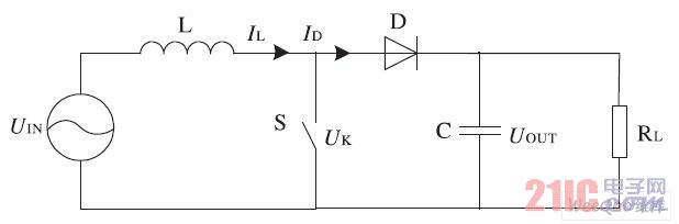
Figure 1 boost converter circuit structure 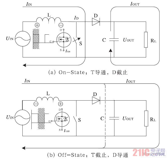
Figure 2 Principle of the boost converter: turn-on phase (a) and turn-off phase (b) 
The input voltage is recorded as UIN and the output voltage is recorded as UOUT. If S is turned on, the input supply voltage will be absorbed by the inductor and there will be no voltage drop across S. If the D-on time is long enough, the inductor L can be seen as a short circuit and there is no voltage drop. Ignoring the forward voltage drop of the diode, the relationship between UIN and UOUT is derived as follows: 
Since D1 <1, the output voltage is greater than the input voltage. In addition, the two switches also regulate the output voltage. If the output voltage is higher than 19 V, the output voltage must be forced to drop. S is turned on and the D cutoff causes the capacitor and load to be removed from the rest of the circuit. At this point, the capacitor acts as a power source for the load. The discharge reduces the voltage across the capacitor, which reduces the output voltage. If the output voltage is below 19 V, the output voltage must be increased. S is turned off, D is turned on, and current flows through diode D, capacitor C, and load RL to form a loop. As the current charges the capacitor, the voltage across the capacitor increases, causing the output voltage to increase. 
The above equation shows the relationship between the output voltage UOUT and the power tube switching time. Due to the short tOFF time, low-power diodes and capacitors are used so that they do not exceed the safe operating area. Otherwise, the device may overheat and be damaged. The current and voltage waveforms of this boost converter are shown in Figure 3. 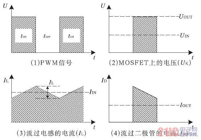
Figure 3 Voltage and current waveforms at 50% duty cycle 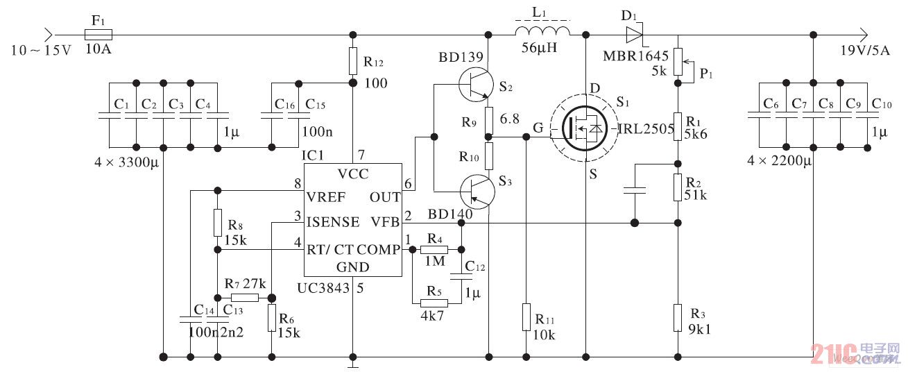
4 Conclusion
2) Non-destructive Smart Pulse Restorer
8 Pulse restore channels for different capacity of batteries: 36Ah~75Ah, 75Ah~120Ah, 100Ah~300Ah. Selecting the suitable range can be ensure better protection of battery plate in restore working, and extend batteries life up to 2 times than before. It is also called Battery Pulse Desulfurizer, Battery Refresher or Sulfuric Crystal Cleaner and maintainer
3) Discharge Capacity Tester
4 discharge channels of detecting and capacity testing , with discharge current range: 0A~ 20A(Output discharge current can be adjusted continuously and input power accurately.), current precision: ±1% and voltage error: 0.05V. Choose the right ranges of discharge current in order to improve the efficiency of battery recovery, Prevent deep discharge and make sure the plates to be protected better.