1 Introduction In this paper, based on the 0.35 micron N-well process, a fully differential chopper op amp circuit powered by a single power supply is designed. At the same time, in order to reduce the residual voltage offset, T / H (track-and-hold) demodulation technology is used. When the circuit works at the chopping frequency of 150KHz, the input equivalent noise reaches 31.12nV / Hz.
Lawn lamp design mainly exterior and downy lamplight add security for urban green space landscape and beautiful, and generally has the characteristic such as easy installation, adornment sex is strong, can be used for park, garden villas, square, greening, greening of the place such as decorative lighting.
Product features
1. The lamp body is made of aluminum alloy with the column in high strength
2. Static powder spray coating process with many different colors for options
3. The LED lighting modules give the highest lighting output to produce the optiumum light beam control and visual comfort.
4. Protection:IP54
5. Heart radiation structure design for lighting assembly,greatly enhancing the stability and lifespan of the lamp.
6. LED Lighting columns with RGB and change program comprising artistic design elements.
7. Reasonable design for assembling and disassembling,convenient for installation and maintenance.
Lawn Lamps,Solar Lawn Lamps,Outdoor Lawn Lamps,Gas Lawn Lamps Jiangsu chengxu Electric Group Co., Ltd , http://www.chengxulighting.com
In the design of op amp circuits for Class D audio amplifiers, low harmonic distortion (Total Harmonic distorTIon) and noise of the signal pose challenges to the design of the op amp. For audio signals in the 20 to 20KHz range, the distortion of the op amp is mainly caused by voltage offset and low-frequency 1 / f noise. The relatively high 1 / f noise and voltage offset of the CMOS process make this problem particularly serious. When the required offset voltage of the circuit is less than 1mV and the input equivalent noise is less than 100nV / Hz. Ordinary CMOS op amps are difficult to meet demand. The common static offset nulling techniques, such as trimming, can eliminate the effect of voltage offset, but they cannot reduce 1 / f noise. The best way to solve this problem is to adopt dynamic offset-cancellaTIon techniques, such as automatic zero stabilization and chopping techniques. Auto zero TIechnique is to sample low-frequency noise and offset, and then subtract them from the instantaneous value of the signal at the input or output of the op amp to reduce offset and noise. Since the auto-zeroing technology uses the principle of capacitor sampling, it is easy to fold broadband thermal noise into the baseband frequency during circuit operation, and the wider the bandwidth of the op amp, the more noise on the sampling capacitor, usually up to 70nV / Hz. Chopper Technique uses modulation and demodulation principles to move low-frequency noise and offset to the high-frequency part, and uses low-pass filtering to filter out. Since there is no aliasing of thermal noise, the noise voltage of the op amp is more stable than automatic Zero technology is lower. However, the impact of the chopper switch charge injection and charge feedthrough effects can still produce a residual offset of about 100uV. And the use of chopper switches will increase the thermal noise level of the device.
2 The working principle of chopper op amp
The principle of the chopping op amp is shown in Figure 1, where Vin is the input audio signal, which is modulated by a chopping switch with a frequency of fch and an amplitude of 1. According to the Nyquist sampling principle, in order to avoid aliasing of the input signal, fch must be much greater than 2 times the signal bandwidth. 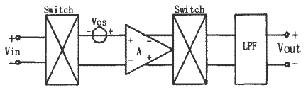
Figure 1 The principle of chopping op amp
After modulation, the signal is moved to the odd harmonic frequency of the chopped square wave. This signal is amplified by an operational amplifier with a gain of Av. At the same time, the input noise and input offset voltage of the op amp are also amplified by the op amp. The output of the op amp is modulated by a chopping switch of amplitude 1 and frequency fch. The output signal is: ![]()
It can be seen from equation (1) that after the second chopping, the input audio signal is demodulated to a low frequency band, and the voltage offset and low frequency noise of the op amp are moved to the high level of the chopped square wave after only one modulation. On the frequency odd harmonics, after low-pass filtering, the high-frequency components in the output signal are filtered out, and the low-frequency components are restored to the audio signal, thereby achieving accurate amplification of the audio signal.
Fourier analysis of the output signal, the final input noise spectral density (PSD) of the op amp is: ![]()
The coefficient K is related to the noise parameters of the process.
3 Design of op amp circuit
The chopper amplifier designed in this paper is a CMOS fully differential circuit structure. It consists of four parts: chopper switch, main operational amplifier circuit, output stage and common mode feedback circuit. The working voltage of the circuit ranges from 2.5V to 5.5V. The circuit structure of the chopper operational amplifier is shown in Figure 2. 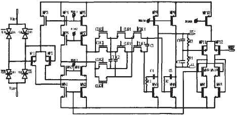
Figure 2 Chopper op amp circuit structure
The input chopper switch completes the modulation of the audio signal. The chopper switch introduces residual voltage offset on both the upper and lower edges of the clock. Figure 3 shows the waveform of the residual offset voltage at zero input. 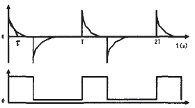
Figure 3 (a) Residual offset voltage (b) Chopping signal 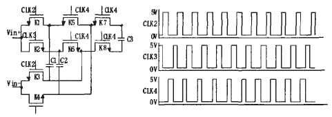
Figure 4T / H demodulation and control timing
By analyzing the characteristics of the CMOS switch, it can be concluded that the equivalent input residual offset voltage is Vos, rmts = 2Vspiketfch, where t is the time constant of the MOS switch. From this equation, it can be seen that there are three methods to eliminate the residual voltage offset:
1. Reduce the chopping frequency:
2. Reduce the input resistance;
3. Reduce the charge injection effect of the chopper switch.
Since the corner frequency of the 1 / f noise of the MOS tube is generally above tens of KHz, reducing the chopping frequency cannot modulate the 1 / f noise well, and the input resistance is only related to the internal resistance of the signal source, which is difficult in the design The input resistance is reduced, so only the charge injection effect of the switch can be reduced. For this reason, the input chopper switch uses a complementary clock structure and uses the smallest line width in size. On the one hand, it can reduce the on-resistance of the transmission and provide a larger voltage swing; on the other hand, it reduces the charge injection and feedthrough. The effect is to reduce the residual voltage offset. Considering that the PMOS tube has better 1 / f noise characteristics than the NMOS tube, the input tubes MP1 and MP2 use large-area PMOS tubes, which can not only reduce the voltage offset caused by the device mismatch, but also reduce the transistor 1 / f noise. The corner frequency improves the noise characteristics of the op amp.
In order to reduce the residual voltage offset less, the output of the fold-cascode op amp uses T / H demodulation technology. The circuit structure and timing are shown in Figure 4. The working principle of the circuit: K1 ~ K4 is closed, K5 ~ K8 is open, the output signal remains on the capacitors C1 and C2 when the signal is tracked, K1 ~ K4 is open, K5 ~ K8 is closed, C1 and C2 The voltage value of is loaded on the load capacitor C3 and summed. Because the voltage on C2 is reversed when superimposed on the load capacitor, the residual voltage offset of the amplifier can be effectively cancelled. Because the demodulator uses high-impedance junction chopping. So you can use a smaller area NMOS tube switch to reduce the impact on the output pole.
The main operational amplifier adopts a fully differential folding cascode structure. In the Class-D structure, due to the frequent opening of the large current of the output power MOSFET, the generated electromagnetic interference (EMI) will form a strong ripple on the power supply. In practical applications It is found that when the chip works at a power supply voltage of 5V, the power supply fluctuation caused by EMI can reach ± ​​2V. The fully differential structure can both improve the power supply rejection ratio and common mode rejection ratio of the op amp, and reduce the influence of power supply noise and common mode noise And the mirror pole is avoided, so it can still show stable characteristics for a larger bandwidth.
In order to provide higher gain and voltage output swing, a common source op amp output stage is added after fold-cascode. After the use of secondary op amps. Analyze the frequency stability of the op amp. Without considering the effect of the chopper switch for the time being, it can be concluded that the circuit has at least three LHP poles, which are the main pole Wp1 introduced by the miller compensation capacitor and the output pole Wpout generated by the output filter capacitor. For the first non-dominant pole, and the non-pole Wp3 introduced by the folded-cascode (the drain of MN1 and the source of MN3), the relationship between the three is Wp1
The common mode feedback circuit is composed of MN7 ~ MN10, MP10-MP12, the input end is connected to the reference voltage of VDD / 2, and the other end is connected to the common mode output of the main op amp. The common mode detection circuit is composed of resistance and capacitance. After the error amplification, the bias current of the main op amp is adjusted.
4 Simulation results and layout design
At SMIC O. Under 35 micron N-well technology. The cadence spectre tool was used to simulate and analyze the circuit designed in this paper. Among them, the process parameters of each device are typical, the power supply voltage is 5V, the input signal is a standard sine wave with an amplitude of 10uV and a frequency of 1KHz, and the chopping frequency is fch = 150K. The simulated waveforms are shown in Figures 5 and 6. 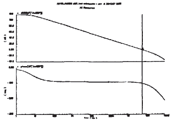
Fig. 5 Amplitude frequency to phase frequency characteristic curve of operational amplifier 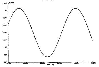
Figure 6 Chopper output waveform
As can be seen from Figure 5, under typical conditions, the main pole of the op amp is within 10HZ, and the phase margin is about 75 degrees. Can fully guarantee the stability of the operational put under various comer conditions. From the input fn waveform, the residual voltage spike caused by chopping has also been significantly improved. Table 1 shows the open loop simulation results of the op amp.
Table 1 Open-loop simulation results of op amp 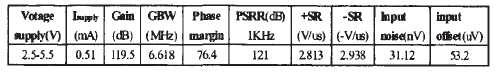
The layout of the circuit adopts SMIC 0.35um process rule design and optimizes the layout. The substrate ground uses a fully enclosed double gardring, which effectively reduces the coupling noise of the substrate. The differential pair uses a dummy gate common centroid matching to reduce input voltage offset. In addition, in order to reduce the interference of the peripheral circuit to the op amp, the filter capacitors of the latter stage are scattered around the op amp circuit. The optimized layout area is 0.24mm × 0.34mm, and the overview is shown in Figure 7. 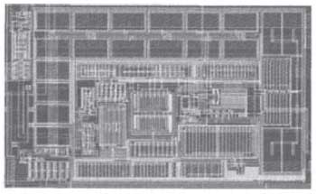
Figure 7 Layout
5 Conclusion
The 1 / f noise and voltage offset of the class D audio amplifier have a direct impact on the distortion and noise performance of the signal, especially when the input signal is zero. The background noise is most obvious. By using a fully differential chopper op amp circuit and T / H demodulation technology effectively reduces the low frequency noise and voltage fire of the system. Tests on the chip after tapping show that this circuit has greatly improved the noise performance of Class-D.
The author of this article is innovative: the use of fully differential chopper op amp circuits and T / H demodulation technology effectively reduces the low-frequency noise and voltage offset of class D audio systems.
Economic benefits of the project: The project has been successfully taped. According to the data from Forward Concepts lnc, the total output value of Class D audio power amplifiers in the world in 2008 was as high as US $ 800 million. 