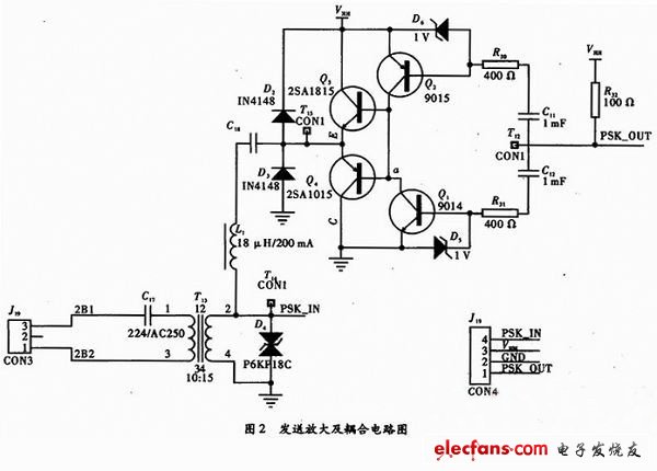
Abstract: The complexity of low-voltage power line transmission characteristics and the variability of interference signals during transmission make its promotion limited. According to the principle of high and low frequency circuit, combined with modern communication and digital signal processing technology, the peripheral dedicated circuit of power line carrier communication, including transmission drive circuit, coupled reception and AGC system, is designed to solve the problem of receiving and transmitting carrier signals. . Keywords: power line carrier communication; coupling; AGC system Power line carrier communication has attracted much attention due to its potential economic benefits and broad application prospects. However, due to the complexity of low-voltage power line transmission characteristics and the variability of interference signals during transmission, its promotion is limited. The low-voltage power line carrier communication module includes a transmission amplifying circuit, a coupled receiving and ACE system, a filtering unit, a modem chip, and the like, as shown in FIG. 1 . The filtering unit and the modulation and demodulation unit integrated chip are designed. For power line communication, the available communication frequency is 60-150 kHz, the carrier frequency band bandwidth is 4 kHz, the transmission information is small, the delay requirement is not high, and the anti-interference requirement is high. According to the high and low frequency circuit principle and digital communication Principle, the power line carrier communication module peripheral dedicated circuit, transmission amplifying circuit, coupled receiving and ACE control circuit are designed to better solve the problem of receiving and transmitting carrier signals. 1 Design of transmit amplification coupling circuit The peripheral circuit of this part completes the adjustment amplification and coupling function before the modulation signal is transmitted. Since the maximum output level of the FPGA pin is 3.3 V, and the signal is coupled through the transmission and reception, the attenuation is large after transmission on the power. Therefore, the modulated signal needs to be properly amplified before being coupled to the power line. on. The transmission amplification and coupling circuit is shown in Figure 2. Measurements show that the impedance of the power line is between 0.5 and 80 Ω, and its impedance depends mainly on the size of the electrical load, the structure of the line, and the impedance of the distribution transformer. Since the impedance characteristics of the distribution line structure and the distribution transformer are relatively stable, the magnitude of the power load has a large influence on the variation of the power line impedance. Due to the randomness of the electric load, the main performance is that the electric load changes at different times, that is, the time variation of the impedance. Studying the input impedance of the power line, in order to improve the transmission power of the signal and the input power of the useful signal, it is typical to set the input impedance of the power line to 5 Ω in the analysis transmission circuit. In the interface circuit with the power line, a high-power voltage regulator tube and a resistor are used to form a limiter circuit for protection. It prevents the system from being disturbed by transient overvoltages such as strong lightning impulses. The transmitting circuit is mainly composed of a power amplifier. The function of the power amplifier is to power amplify the square wave signal output from PSK_OUT. In order to improve the transmission power, the output stage is a heterogeneous composite tube single-supply quasi-complementary class B push-pull circuit. The preamplifier uses 9014 and 9015 pairs of tubes, and the D5 and D6 two 5.1 V regulators protect the triode from reverse breakdown. Because the current is relatively large, the 2SA1015 and 2SA1815 pairs with relatively high current resistance are used. Similarly, the carrier signal from the line is coupled to the carrier receiving circuit through the coil, and the D4 bidirectional Zener diode protects the device from large voltage damage. Coupling coils are more important. Choose a 10:15 coil. The high voltage and low voltage of the connector are separated. The high voltage part is connected to the 220 V interface. The low voltage is PSK_OUT, GND, VHH and PSK_IN according to the pin sequence. The coupling circuit is designed to achieve reliable carrier communication using power lines, and its analysis and design are the key to the problem. The difficulty lies in: (1) the loading efficiency of the carrier signal is required to be high. (2) It is required that the power frequency signal of the power grid of 50 Hz cannot cause too much interference to the carrier communication system. A power matching and gain balancing circuit that effectively reduces the low impedance effects of the low voltage power line is designed to couple the signal to the power line with a transmission band of 0.1 to 30.0 MHz. In order to achieve the maximum power transmission of the network signal, the circuit design must consider the impedance characteristics of the 220 V line side, T100 is the signal coupling transformer, and the impedance of the 220 V line side is about 30 Ω. Then determine the turns ratio or impedance ratio of the coil primary. Finally, the output matching resistor of the power amplifier is designed. In order to prevent lightning and switching transients on the low-voltage power line, permanent damage to the circuit components is required, and special protection measures are required. As shown in the coupling section of Figure 2, the transformer provides a linear transmission function for the spread spectrum carrier signal of 100 to 400 kHz. The function of the capacitor is to prevent the 50 Hz power frequency from entering the transformer T, limiting the transformer current to avoid the transformer iron. The core is saturated. The input channel should be connected to a surge protection diode 5KP18C, which is connected to the pre-stage filter circuit after being isolated by the resistor and connected to the diode clamp circuit. When the load on the power line changes, the power line will generate a large noise or even a large amplitude spike, which will cause greater harm to the latter circuit after being coupled. Therefore, after adding a surge protection diode, this noise can be well filtered and the latter circuit can be protected. Two diodes are connected behind for overvoltage protection.
Active GPS Antenna Description:
This is a high quality Car GPS Antenna for After-Market/Stock GPS Navigation with SMA Aerial Connection Port. To help your GPS Navigation System to get stronger & stable signal.
Center Frequency: 1575.42MHz-3MHz / 1575.42MHz+3MHz, Length: 9feet (3m), Weatherproof: 100% Weatherproof, DC current: 10mA Max, LNA Gain(Without cable): 28dB.
Active Gps Antenna Specifications:
Active Gps Antenna Pictures:
Active GPS Antenna,Trimble GPS Antenna,Waterproof Active GPS Antenna,Signal Receiver Active Gps Antenna Shenzhen Yetnorson Technology Co., Ltd. , http://www.yetnorson.com
Easy to install: the antenna has a magnetic base which can stick to any metal surface or just put it under windshield glass.
GPS Active Antenna SMA male connector
Length: 9 feet (3m)
Center Frequency: 1575.42MHz-3MHz / 1575.42MHz+3MHz
LNA Gain(Without cable): 28dB
Noise Figure: <1.5dB
V.S.W.R: <2.0
DC current: 10mA Max
Mounting: Magnetic base
Housing: Black
Working Temp: -40C~+85C
Humidity: Humidity 95%~100%RH
Weatherproof: 100% Weatherproof
Voltage: 3~5V

