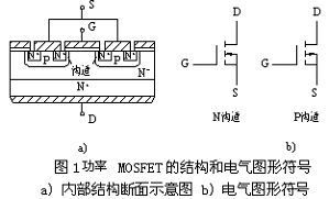
1. Overview The term MOSFET stands for Metal-Oxide-Semiconductor Field-Effect Transistor. It is a type of transistor that uses an electric field to control the flow of current through a semiconductor. In its basic form, it consists of three layers: a metal gate, an oxide layer, and a semiconductor (usually silicon). This structure allows the device to act as a switch or amplifier in electronic circuits. Power FETs are categorized into junction types and insulated gate types. The insulated gate type is commonly referred to as the MOSFET, specifically known as the Power MOSFET. Junction power field effect transistors are generally called Static Induction Transistors (SIT). The key feature of a Power MOSFET is its ability to control the drain current using a gate voltage, making it ideal for applications where high efficiency and fast switching are required. Its advantages include a simple driving circuit, low driving power, fast switching speed, and high operating frequency. However, it has limitations such as lower current capacity and voltage rating compared to other devices like GTRs (Giant Transistors), typically suitable for power electronics up to 10 kW. 2. Structure and Working Principle of Power MOSFET Power MOSFETs can be classified based on their conductive channel, which includes P-channel and N-channel types. They can also be divided into depletion type and enhancement type. In depletion type, a conductive channel exists even when the gate voltage is zero, while in enhancement type, the channel is formed only when the gate voltage exceeds a certain threshold. Most power MOSFETs are N-channel enhancement type due to their superior performance characteristics. 2.1 Internal Structure and Electrical Symbol The internal structure and electrical symbol of a power MOSFET are illustrated in Figure 1. When turned on, only one type of carrier (either electrons or holes) participates in conduction, making it a unipolar device. The conduction mechanism is similar to that of small power MOSFETs, but the structure is quite different. Small power MOSFETs are lateral devices, while power MOSFETs usually adopt a vertical structure, known as VMOSFET (Vertical MOSFET), which significantly improves the resistance and current handling capability of the device. Depending on the vertical conduction structure, power MOSFETs can be further divided into VVMOSFET, which uses a V-groove for vertical conduction, and VDMOSFET (Vertical Double-diffused MOSFET), which has a double-diffused structure. This article mainly discusses the VDMOS device as an example. Power MOSFETs are multi-integrated structures. For instance, International Rectifier's HEXFET uses a hexagonal unit, Siemens' SIP MOSFET uses a square unit, and Motorola's TMOS uses a rectangular unit. These configurations enhance the performance and reliability of the device. 2.2 Working Principle of Power MOSFET When the power MOSFET is in cutoff mode, a positive voltage is applied between the drain and source, but the gate-source voltage is zero. This causes the PN junction J1, formed between the P base region and the N drift region, to be reverse biased, preventing current from flowing between the drain and source. In the conducting state, a positive voltage UGS is applied between the gate and source. The gate is insulated, so no gate current flows. However, the positive gate voltage pushes the holes in the P region below it and attracts the minority electrons in the P region to the surface. When UGS exceeds the threshold voltage UT, the electron concentration on the P region surface becomes higher than the hole concentration, causing the P-type semiconductor to invert into an N-type, forming an inversion layer and an N-channel. This allows current to flow between the drain and source. 2.3 Basic Characteristics of Power MOSFET 2.3.1 Static Characteristics The transfer characteristic of a MOSFET describes the relationship between the drain current ID and the gate-source voltage UGS. When ID is large, this relationship is approximately linear, and the slope of the curve is defined as the transconductance Gfs. The output characteristic, or volt-ampere characteristic, shows three regions: cutoff, saturation, and unsaturated. The power MOSFET operates in a switching state, toggling between the cutoff and unsaturated regions. There is a parasitic diode between the drain and source, which turns on when a reverse voltage is applied. The on-resistance of the power MOSFET has a positive temperature coefficient, which is beneficial for current sharing when devices are connected in parallel. 2.3.2 Dynamic Characteristics The dynamic characteristics of a MOSFET involve its switching process. Key parameters include the turn-on delay time (td(on)), rise time (tr), turn-on time (ton), turn-off delay time (td(off)), fall time (tf), and turn-off time (toff). These times are influenced by the charging and discharging of the input capacitance (Cin). Reducing the internal resistance of the drive circuit can improve the switching speed. Since the MOSFET is controlled by multiple sub-transistors, it does not suffer from the minority carrier storage effect, allowing for very fast turn-off processes, with switching times between 10 and 100 ns and operating frequencies above 100 kHz. 2.3.3 Switching Speed The switching speed of a MOSFET is closely related to the charging and discharging of Cin. While users cannot reduce Cin, they can reduce the internal resistance of the drive circuit to decrease the time constant and increase the switching speed. Although the MOSFET requires some driving power during the switching process, its high input impedance and lack of minority carrier storage make it highly efficient. 2.4 Improving Dynamic Performance In addition to considering voltage, current, and frequency, it is essential to protect the device from damage during transient conditions. Unlike thyristors, which have large capacitances and poor dv/dt capabilities, power MOSFETs have much better dv/dt and di/dt capabilities, often measured in nanoseconds. However, they still have dynamic performance limitations due to their internal structure, including parasitic elements such as diodes and transistors. These factors must be considered when analyzing the dynamic characteristics of the MOSFET. 3. Principles and Performance Analysis of High Voltage MOSFETs MOSFETs play a critical role in various power conversion systems, especially in high-frequency applications. They offer high-speed operation, low switching loss, and low driving loss. In low-voltage applications, MOSFETs have no competition, but as the breakdown voltage increases, the on-resistance rises rapidly, leading to trade-offs between rated current, on-resistance, and cost. Despite these challenges, high-voltage MOSFETs remain widely used, although their conduction losses dominate, limiting their application in high-power systems. 3.1 Methods to Reduce On-Resistance of High-Voltage MOSFETs The on-resistance of high-voltage MOSFETs is primarily determined by the epitaxial layer resistance. As the breakdown voltage increases, the epitaxial layer becomes thicker and more resistive, increasing the on-resistance. To address this, innovative designs such as COOLMOS have been introduced, which use built-in lateral electric fields to separate the blocking voltage function from the on-resistance function, reducing the overall resistance and improving performance. 3.2 Main Features of Built-In Lateral Electric Field MOSFETs COOLMOS technology has significantly reduced the on-resistance of high-voltage MOSFETs, resulting in lower conduction losses and improved thermal performance. These devices also exhibit enhanced switching characteristics, faster turn-off times, and better avalanche and short-circuit protection. Their design allows for more efficient heat dissipation and greater reliability in demanding applications. 3.3 Development Status of High-Voltage MOSFETs with Built-In Transverse Electric Fields Following the introduction of COOLMOS in 1988, several manufacturers have developed similar technologies, leading to significant improvements in performance. These devices are now widely used in high-voltage applications, offering superior efficiency, reliability, and cost-effectiveness compared to traditional MOSFETs. 3.4 Comparison Between COOLMOS and IGBT COOLMOS offers advantages over IGBTs in terms of lower conduction and switching losses, faster switching speeds, and better thermal management. While IGBTs are still used in high-power applications, COOLMOS provides a more efficient alternative for many modern power electronics systems, particularly those requiring high-frequency operation and low-loss performance. 4. Power MOSFET Drive Circuit Power MOSFETs are voltage-controlled devices with high input impedance, making them ideal for applications where fast switching and low driving power are required. However, their inter-electrode capacitance can affect performance, necessitating careful design of the drive circuit. A well-designed drive circuit ensures fast switching, reliable operation, and protection against interference and overvoltage conditions. 4.1 Introduction and Analysis of Several MOSFET Drive Circuits Various drive circuits are used to control power MOSFETs, including non-isolated complementary circuits, isolated circuits, and integrated chip-based solutions. Each type has its own advantages and limitations, depending on the application requirements. Non-isolated circuits are simple and cost-effective, while isolated circuits provide better safety and noise immunity. Integrated solutions offer compact designs and advanced features, making them suitable for complex power systems. Fire Resistant Wire,Refractory Wire,Fire Resistant Insulated Wire,High Temperature Cable JIANGSU PENGSHEN HIGH TEMPERATURE WIRE CABLE CO., LTD. , https://www.pengshencable.com