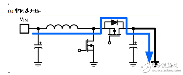
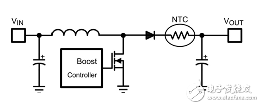
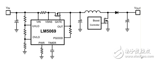
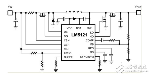
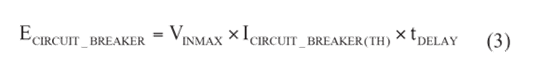
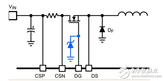
Between the engineers' emphasis on power protection requirements, the boost conversion stage provides system advantages through the high voltages available on local loads. Output short-circuit faults, overload conditions, other fault conditions, and high capacitance at startup can severely increase the input supply load, or cause input power failure, and damage the load. The load itself is very demanding and requires even higher voltages than the voltage supplied by the main input supply. These conditions and requirements cause the input supply to be over-engineered or overburdened, especially when boost loads are required. Boost converters are a common choice for higher voltage loads, and the problem is that they do not provide system protection for downstream circuits. This is caused by the inherent conduction path from input to output; this path further increases the burden on the mains and reduces system reliability, especially in faulty or overload conditions. For example, in a low voltage battery powered system, the voltage required by the load can be higher than the voltage that the main power supply can provide. Industrial systems that provide fixed bus power through cables and communication systems with high efficiency power amplifiers often require a boost voltage from a wide input range DC/DC regulator. A boost power supply has certain system advantages. In systems with larger wiring harnesses, the high voltage reduces the wire gauge required to deliver the total power. The automotive industry has analyzed the problems caused by expensive, bulky cable lines by delving into 48V batteries. Systems with high power amplifiers such as RF transmitters have found ways to increase efficiency and increase output power density from the high supply voltage operation of new transistors. Some mission critical systems need to store energy through capacitive energy storage, which requires less capacitance at higher voltages (E = 1/2 * C * V2). A boost boost circuit enables smaller solution sizes. If the boost converter's own limitations are not taken into account, it will reduce system reliability and increase system cost, resulting in over-design of other parts of the system. A boost circuit itself has a conduction path from input to output (Figure 1). Even when the converter is off, current can flow to the output through the boost diode or synchronous power FET body diode. (a) Non-synchronous boost (b) Synchronous boost In the case of heavy capacitive loads, the mains or battery must be able to withstand the burden of inrush current because the boost converter does not provide any load isolation. When there is no separate current limiting mechanism, the main power supply will exceed the requirements. In systems such as alarm systems that require a backup battery, uncontrolled current consumption can affect battery reliability or require a larger capacity battery. Even the expected heavy load conditions can cause a limited power supply (such as a battery) to drop power; the drop is enough to temporarily power down circuits on other system voltage rails and cause an unexpected system restart. In the absence of inrush limits or coordinated power sequencing, the power bus limits the number of modules that can be allowed based on the maximum supply current capability. Faulty loads such as motor stalls that occur when an overload occurs can draw large currents. The solenoid used in the ejector is another example of a load that can cause a short circuit fault. The pluggable module of the motor may require a boost voltage rail (provided by the main system) to save space and cost in a detachable assembly, but also draws too much current from the mains during hot swapping. Unprotected boost converters are not equipped with equipment to mitigate these risks; it simply adds the burden to the power supply. Designers often solve this problem by over-engineering or over-utilizing the mains, but some simple limitations and protection techniques can save system cost and increase reliability, even when the boost load has failed. Protection method The simplest current limiting system configuration uses a negative temperature coefficient (NTC) thermistor (Figure 2). With the high impedance of cooling, initially, the NTC limits the inrush current during startup. As the self-heating generated by its own power dissipation increases, the impedance decreases, causing more current to flow. The advantage of this approach is its simplicity and the ability to provide a low cost protection solution. However, when implementing this system configuration in a harsh environment, the disadvantages will emerge. In environments with large temperature changes such as car engine compartments, the ambient temperature will become very high, which will reduce the initial impedance of the NTC and generate excessive inrush current if the entire environmental operating conditions are not carefully managed. In the event of a reboot, the NTC device may not cool down until the next power up. The output capacitor may be fully discharged, but due to the slower heat dissipation rate, the NTC's limiting function for inrush current is minimized. In addition, if a load short circuit fault occurs, the NTC will no longer be able to limit the current higher than the supply current under the selected nominal operating conditions. Finally, the NTC method is effective for single-function protection, but it is limited when it is used as a passive component. Figure 3. Active Inrush Current Limit Using Hot Swap Now let's look at active limiting devices such as MOSFETs: it requires a control circuit similar to an inrush limit controller, also known as a hot-swap controller or electronic fuse. Although this is an additional integrated circuit (IC) in front of the controller, many such controllers (Figure 3) feature programmable inrush limiting to ensure that the MOSFET remains in the safe operating area (SOA) while using a Current and voltage control loops to control the inrush rate. SOA monitors the long-term reliability of critical protection devices. In addition, the inrush controller may have two current thresholds: one for the standard inrush limit and the second for the severe overcurrent condition to perform the breaker function. A significant advantage of this implementation is the ability to implement advanced protection features; however, the cost and complexity of this solution is often greater than that of passive methods. The third protection option is a boost controller with an integrated inrush limit. Since the boosted high-side component (freewheeling diode or synchronous MOSFET) cannot be reversed, this method still requires an additional MOSFET as a protection device. However, as shown in Figure 4, integrating boost and protection control into one IC helps reduce solution complexity and size compared to hot-swap controller methods while providing many additional protection features. Figure 4. Boost controller with integrated inrush current limit. Choose a MOSFET for the worst case Any one of the limiting methods requires careful design to ensure that the solution is robust and durable, especially with regard to power consuming devices. When using MOSFETs, be sure to take into account the safe working area of ​​the device. Setting the current is just one of the parameters to consider. When selecting a MOSFET, factors such as the peak turn-off voltage (drain/source voltage) and the length of time that the MOSFET will be in an extreme combination of conditions need to be taken into account. Depending on the system design requirements, use the equation below to help select a MOSFET with sufficient energy by calculating the peak energy on the device under these conditions (inrush, output short, and sudden circuit disconnect). The charging energy for the influx of precautions is: it's here: EINRUSH = Output capacitor charging power in J. COUT = maximum output capacitance value in F. VINMAX = maximum input supply voltage in V. Although the worst case of the output capacitor charging current looks similar to the short circuit condition at first, the true short circuit fault condition on the MOSFET is more stringent. The short-circuit energy that the MOSFET must withstand depends on: it's here: ESHORT = short circuit protection energy in J. IINRUSH(TH) = Inrush current limit threshold in A. tDELAY = delay time in seconds. The selected protection controller may have a fail-safe circuit breaker current threshold that triggers an immediate disconnection of the input. The calculation of the energy for the circuit breaker is similar to the short circuit condition, but with a different current threshold set by the protection controller (if any). The MOSFET worst case tolerable energy is calculated from the controller's response or delay time. it's here: ECIRCUIT_BREAKER = Circuit breaker protection energy in J. ICIRCUIT_BREAKER(TH) = Circuit breaker threshold current in A. One thing to keep in mind is that using MOSFETs for protection can achieve fast response to inrush or fault conditions, and proper voltage buffering should be performed at the output of the MOSFET to ensure that the device used for protection does not go downstream. The circuit has a negative impact. When using a boost circuit, the first in-line component after the protection device is the main inductor. A freewheeling diode manages any voltage ringing between the protection MOSFET and the inductor. It only conducts when the protection switch is quickly turned off, especially when the circuit breaker is on the left side of the inductor (Figure 5). Figure 5. Input voltage transient suppression circuit. Other protection features The retry timer may be another feature you will consider when choosing a protection controller. This protection feature is also known as discontinuous mode. If the device experiences an intermittent overcurrent fault, automatic retry may be more beneficial to the system without requiring an entire system restart. The chopping mode allows the protection controller to turn on the MOSFET and wait for a certain period of time to resolve the fault and then retry by initiating the inrush control sequence. If the fault persists, a controller may retry indefinitely or after a certain number of retries. A second advantage of using a MOSFET as a protection device is that an original input overvoltage protection circuit (/) is implemented. By connecting an appropriately selected Zener diode to the gate of the MOSFET, the gate-to-source voltage of the FET is clamped by the diode, which causes the MOFET to be pulled back to the resistor operation as the supply voltage increases. The breakdown voltage of the diode sets a valid output voltage clamp value. The MOSFET operates as a linear regulator within the resistor region, but one thing to note is that the maximum clamp time allowed is limited by the MOSFET properties. references 1. Download the data sheet: LM5121, LM5069 2. Design a Fault Protection Circuit with Wide VIN LM5121, Application Report (SNVA726), Texas Instruments (TI), January 2015 3. LM5060 High Side Protection Circuit with Low Quiescent Current (SNVS628), Texas Instruments, April 2013 4. CSD19536KCS 100V N-Channel NEXTFETTM Power MOSFET (SLPS485), Texas Instruments, October 2014 5. Robust and hot-swappable design, application report (SLVA673), Texas Instruments (TI), November 2014 6. GaN devices for high efficiency power amplifiers, T. Kikkawa et al., Fujitsu Science and Technology Journal, Vol. 48, No. 1, January 2012 7. Upgrade 12V power supply on the board will pave the way for 48V power supply, Frost & Sullivan, June 2012 related articles 1. Understand power integrity as a system-wide challenge 2. Power integrity: measure and optimize power-related parameters in the electronic system and eliminate related faults 3. Power system performance requires suitable active and passive components 4. When Bode plot cannot provide us with the correct information 5. Stability criteria of the control system 6. Isolated DC-DC converter topologies key authors within the power density: Texas Instruments (TI), Daniel Braunworth, Eric Lee
The Shackle Insulator is made from high quality porcelain material, The Porcelain Shackle Insulator can endure high amount of temperature and current, Shackle Type Insulator usually used in low voltage distribution network.Such High Voltage Porcelain Shackle Insulator can be used either in a horizontal position or in a vertical position. Shackle insulator can be directly fixed to the pole with a bolt or to the Cross Arm .
We warmly welcome friends both domestic and abroad to visit our company, if you have any questions, please contact with us directly.
Shackle Insulator Shackle Insulator,Shackle Type Insulator,Porcelain Shackle Insulator,High Voltage Porcelain Shackle Insulator FUZHOU SINGREE IMP.& EXP.CO.,LTD. , https://www.cninsulators.com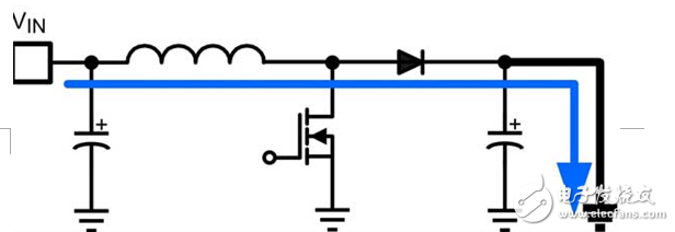


Features
1.The tapered hole of the spool insulator distributes the load more evenly
2.Minimizing the possibility of breakage when heavily loaded
3.Very reliable, with a proven track record. Over 80 years of experience
4.Easier to maintain, can be coated and washed
5.Easy to identify a damaged unit
The following shackle insulators comply with the BS standard, the glaze colour of the insulators are brown, light gray etc..
MAIN DIMENSIONS AND STANDARD PARTICULARS
Type
ED-2(B)
ED-2(C)
Main Dimensions
H
76
80
D
89
80
d
48
50
d1
21
22
R
10
6
Transverse Stength,KN
12.7
13.2
Power Frequence Flashover Voltage
Dry,KV
25
25
Wet,KV
12
12
Net Weight, Each Approx., kg
0.5
0.5
")
")